1999 Sep 20
2
Philips Semiconductors
Product specification
16-bit transceiver with dual enable; 3-state
74ALVCH16623
FEATURES
·
Complies with JEDEC standard
no. 8-1A
·
CMOS low power consumption
·
Direct interface with TTL levels
·
MULTIBYTE
TM
flow-through
standard pin-out architecture
·
All data inputs have bus hold
circuitry
·
Output drive capability 50
transmission lines at 85
°
C
·
Current drive
±
24 mA at 3.0 V.
DESCRIPTION
The 74ALVCH16623 is a high-performance, low-power, low-voltage, Si-gate
CMOS device, superior to most advanced CMOS compatible TTL families.
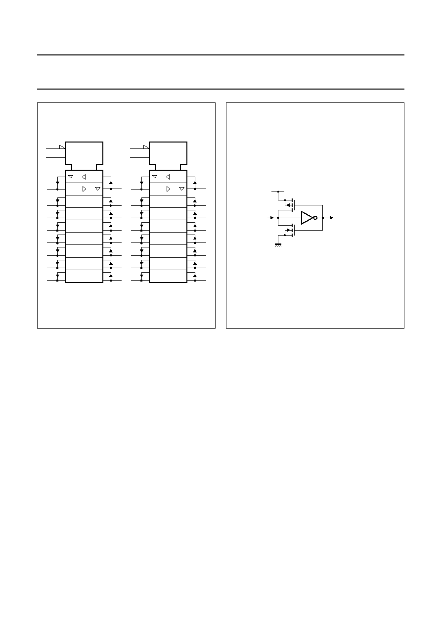
The 74ALVCH16623 is a 16-bit transceiver featuring non-inverting 3-state bus
compatible outputs in both send and receive directions.
This 16-bit bus transceiver is designed for asynchronous two-way
communication between data buses. The control function implementation
allows maximum flexibility in timing. This device allows data transmission from
the A bus to the B bus or from the B bus to the A bus, depending upon the logic
levels at the enable inputs (nOE
AB
, nOE
BA
). The enable inputs can be used to
disable the device so that the buses are effectively isolated. The dual enable
function configuration gives this transceiver the capability to store data by
simultaneous enabling of nOE
AB
and nOE
BA
. Each output reinforces its input in
this transceiver configuration. Thus, when all control inputs are enabled and all
other data sources to the four sets of the bus lines are at high-impedance
OFF-state, all sets of bus lines will remain at their last states. The 8-bit codes
appearing on the two double sets of buses will be complementary. This device
can be used as two 8-bit transceivers or one 16-bit transceiver.
To ensure the high-impedance state during power-on or power-down, OE
BA
should be tied to V
CC
through a pull-up resistor and OE
AB
should be tied to GND
through a pull-down resistor; the minimum value of the resistor is determined
by the current-sinking/current-sourcing capability of the driver.
Active bus hold circuitry is provided to hold unused or floating data inputs at a
valid logic level.
QUICK REFERENCE DATA
Ground = 0; T
amb
= 25
°
C; t
r
= t
f
= 2.5 ns.
Notes
1. C
PD
is used to determine the dynamic power dissipation (P
D
in
µ
W).
P
D
= C
PD
×
V
CC
2
×
f
i
+
(C
L
×
V
CC
2
×
f
o
) where:
f
i
= input frequency in MHz;
C
L
= output load capacitance in pF;
f
o
= output frequency in MHz;
V
CC
= supply voltage in Volts;
(C
L
×
V
CC
2
×
f
o
) = sum of outputs.
2. The condition is V
I
= GND to V
CC
.
SYMBOL
PARAMETER
CONDITIONS
TYPICAL
UNIT
t
PHL
/t
PLH
propagation delay nA
n
, nB
n
to nB
n
, nA
n
C
L
= 30 pF; V
CC
= 2.5 V
2.0
ns
C
L
= 50 pF; V
CC
= 3.3 V
1.9
ns
C
I/O
input/output capacitance
10.0
pF
C
I
input capacitance
3.0
pF
C
PD
power dissipation capacitance per buffer notes 1 and 2
outputs enabled
35
pF
outputs disabled
5
pF
1999 Sep 20
3
Philips Semiconductors
Product specification
16-bit transceiver with dual enable; 3-state
74ALVCH16623
ORDERING INFORMATION
FUNCTION TABLE
See note 1.
Note
1. H = HIGH voltage level;
L = LOW voltage level;
Z = high-impedance OFF-state.
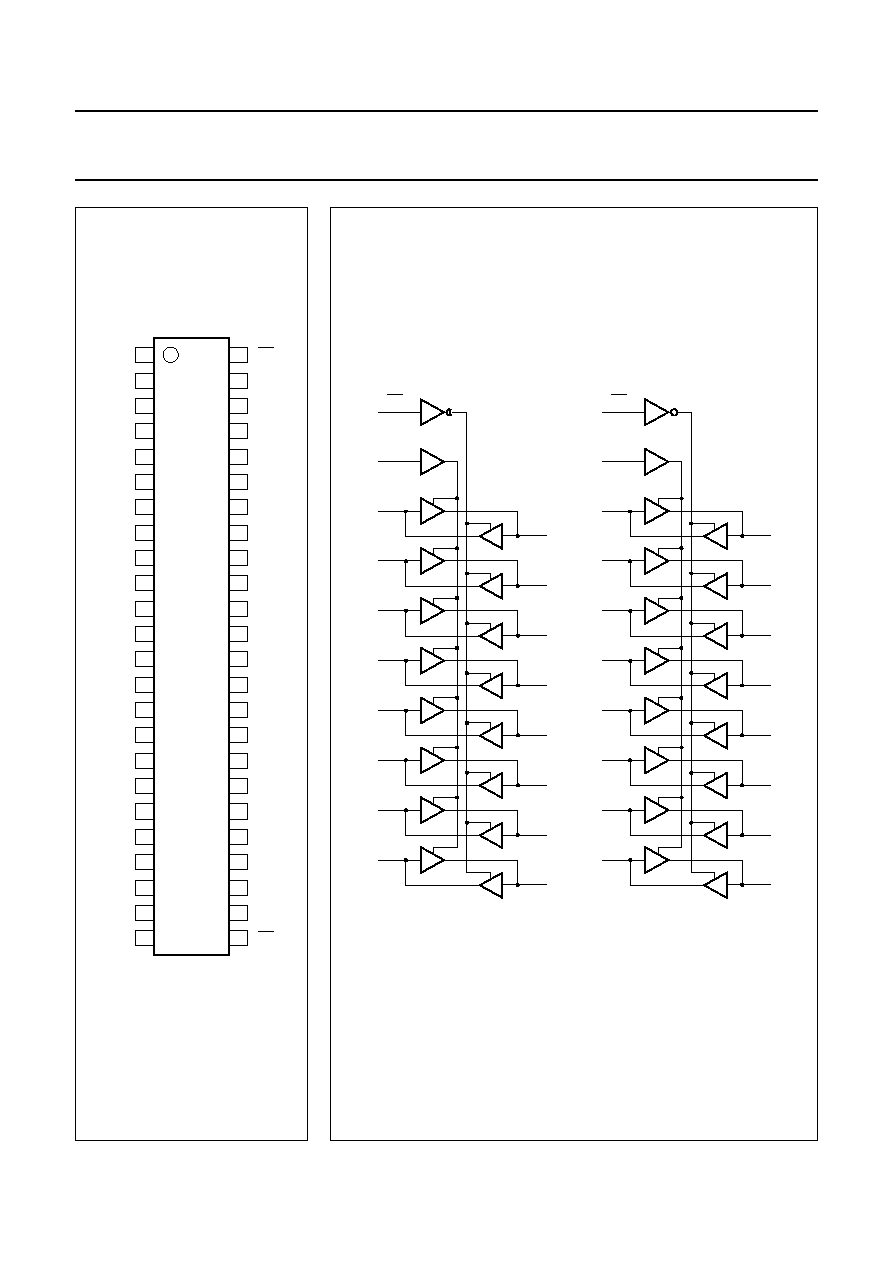
PINNING
TYPE NUMBER
PACKAGE
TEMPERATURE RANGE
PINS
PACKAGE
MATERIAL
CODE
74ALVCH16623DGG
-
40 to +85
°
C
48
TSSOP
plastic
SOT362-1
INPUTS
INPUTS/OUTPUTS
nOE
AB
nOE
BA
nA
n
nB
n
L
L
A = B
inputs
H
H
inputs
B = A
L
H
Z
Z
H
L
A = B
B = A
PIN
SYMBOL
DESCRIPTION
1, 24
1OE
AB
, 2OE
AB
output enable input (active HIGH)
2, 3, 5, 6, 8, 9, 11, 12
1B
0
to 1B
7
data inputs/outputs
4, 10, 15, 21, 28, 34, 39, 45
GND
ground (0 V)
7, 18, 31, 42
V
CC
DC supply voltage
13, 14, 16, 17, 19, 20, 22, 23
2B
0
to 2B
7
data inputs/outputs
25, 48
2OE
BA
, 1OE
BA
output enable input (active LOW)
26, 27, 29, 30, 32, 33, 35, 36
2A
7
to 2A
0
data inputs/outputs
37, 38, 40, 41, 43, 44, 46, 47
1A
7
to 1A
0
data inputs/outputs