
1
PS8702A 09/10/03
Inputs
Outputs
OE
DIR
L
L
Bus B Data to Bus A
L
H
Bus A Data to Bus B
H
X
Z (Isolation)
Product Description
Pericom Semiconductor's PI74LVC series of logic circuits are
produced using the Company's advanced submicron CMOS tech-
nology, achieving industry leading speed.
The PI74LVCC3245A is a non-inverting 8-bit Bidirectional Trans-
ceiver that uses two seperate power supply rails. A-port (V
CCA
) is set
to operate at 3.3V and B-port (V
CCB
) is set to operate from 3.3V to
5V. This allows for translation from a 3.3V to a 5V environment and
vice-versa. This tranceiver is designed for asynchronous two-way
communication between data buses. The direction control input pin
(DIR) determines the dataflow from the A bus to the B bus or from
the B bus to the A bus. The output enable (OE) input, when HIGH,
disables both A and B ports by placing them in HIGH Z condi-
tion.
8-Bit Dual Supply Bus Transceiver with
Configurable Output Voltage and 3-State Outputs
Logic Block Diagram
Product Features
· 2.7V to 3.6V on A-port and 3V to 5.5V on B-port
· Latch-up performance exceeds 200mA Per JESD78
· ESD protection exceeds JESD22
2000V Human-Body Model (A114-B)
200V Machine Model (A115-A)
· Industrial Temperature: 40°C to +85°C
· Packages (Pb-free available):
- 24-pin 173-mil wide plastic TSSOP (L)
(Pb-free & Green available)
- 24-pin 150-mil wide plastic QSOP (Q)
- 24-pin 300-mil wide plastic SOIC (S)
PI74LVCC3245A
B
1
A
1
OE
DIR
B
2
A
2
B
3
A
3
B
4
A
4
B
5
A
5
B
6
A
6
B
7
A
7
B
8
A
8
2
5
3
4
8
6
7
10
9
22
19
21
20
16
18
17
14
15
Truth Table
(1)
Note:
1. H = High Signal Level L = Low Signal Level
X = Don't Care or Irrelevant Z = High Impedance
(3.3V) V
CCA
DIR
A1
A2
A3
A4
A5
A6
A7
A8
GND
GND
VCCB (3.3V to 5V)
NC
OE
B1
B2
B3
B4
B5
B6
B7
B8
GND
24
23
22
21
20
19
18
17
16
15
14
13
1
2
3
4
5
6
7
8
9
10
11
12
Product Pin Description
Product Pin Configuration
Pin Name
Description
OE
3-State Output Enable Inputs (Active LOW)
DIR
Direction Control Input
Ax
Side A Inputs or 3-State Outputs
Bx
Side B Inputs or 3-State Outputs
NC
NO Internal Connect
GND
Ground
V
CCA
,V
CCB
Power

PI74LVCC3245A
8-Bit Dual Supply Bus Transceiver with
Configurable Output Voltage and 3-State Outputs
2
PS8702A 09/10/03
Supply voltage range, V
CCA
and V
CCB
............................
0.5V to +7V
Input voltage range, V
I
(2)
: I/O ports (A-port)
....
0.5V to V
CCA
+0.5V
I/O ports (B-port)
...........
0.5V to V
CCB
+0.5V
Control Pins
.................
0.5V to V
CCA
+0.5V
Input clamp current, I
IK
(V
I
<0)................................................50mA
Output clamp current, I
OK
(V
O
<0)...........................................50mA
Continous Output Current I
O
..................................................±50mA
Continous Current through each V
CC
or GND pin
.....................±100mA
Package thermal impedance,
JA
(3)
: package L...................... 84°C/W
package Q...................... 98°C/W
package S ...................... 79°C/W
Storage Temperature range, T
stg
................................65°C to 150°C
Maximum Ratings
(Above which the useful life may be impaired. For user guidelines, not tested.)
2. This value is limited to 7V maximum.
3. The package thermal impedance is calculated in accordance with JESD
51.
Notes:
Stresses greater than those listed under MAXIMUM RATINGS may cause
permanent damage to the device. This is a stress rating only and func-
tional operation of the device at these or any other conditions above those
indicated in the operational sections of this specification is not implied.
Exposure to absolute maximum rating conditions for extended periods
may affect reliability.
PI74LVCC3245A
8-Bit Dual Supply Bus Transceiver with
Configurable Output Voltage and 3-State Outputs
3
PS8702A 09/10/03
Recommended Operating Conditions
(4)
Note: 4. All unused inputs of the device must be held at the associated V
CC
or GND to ensure proper device operation.
Parameter
Description
V
CCA
V
CCB
Min.
Nom.
Max.
Units
V
CCA
Supply Voltage
2.7
3.3
3.6
V
V
CCB
Supply Voltage
3
5
5.5
V
IHA
High-Level Input Voltage
V
OB
0.1V
or V
OB
V
CCB
0.1V
2.7V
3V
2
3.0V
3.6V
2
3.6V
5.5V
2
V
IHB
High-Level Input Voltage
V
OA
0.1V
or V
OA
V
CCA
0.1V
2.7V
3V
2
3.0V
3.6V
2
3.6V
5.5V
3.85
V
ILA
Low-Level Input Voltage
V
OB
0.1V
or V
OB
V
CCB
0.1V
2.7V
3V
0.8
3.0V
3.6V
0.8
3.6V
5.5V
0.8
V
ILB
Low-Level Input Voltage
V
OA
0.1V
or V
OA
V
CCA
0.1V
2.7V
3V
0.8
3.0V
3.6V
0.8
3.6V
5.5V
1.65
V
IH
High-Level Input Voltage
(Control Pins)
V
OA
0.1V
or V
OA
V
CCA
0.1V,
or V
OB
0.1V
or V
OB
V
CCB
0.1V
2.7V
3V
2
3.0V
3.6V
2
3.6V
5.5V
2
V
IL
Low-Level Input Voltage
(Control Pins)
V
OA
0.1V
or V
OA
V
CCA
0.1V,
or V
OB
0.1V
or V
OB
V
CCB
0.1V
2.7V
3V
0.8
3.0V
3.6V
0.8
3.6V
5.5V
0.8
V
IA
Input Voltage
0
V
CCA
V
IB
Input Voltage
0
V
CCB
V
OA
Output Voltage
0
V
CCA
V
OB
Output Voltage
0
V
CCB
I
OHA
High-level output Current
2.7V
3V
12
mA
3.3V
3V
24
I
OHB
High-level output Current
2.7V
3.3V
12
3.3V
3V
24
I
OLA
Low-level output Current
2.7V
3V
12
3.3V
3V
24
I
OLB
Low-level output Current
2.7V
3.3V
12
3.3V
3V
24
t/v
Input transition Rise or Fall
Rate
10
ns/v
T
A
Operating Free-Air Tem-
perature
40
85
°C
PI74LVCC3245A
8-Bit Dual Supply Bus Transceiver with
Configurable Output Voltage and 3-State Outputs
4
PS8702A 09/10/03
Parameters Description
Test Conditions
V
CCA
V
CCB
Min. Typ. Max. Units
V
OHA
Minimum High Level
Output Voltage (Port A)
I
OH
= 100µA
3V
3V
2.9
3
V
I
OH
= 12mA
2.7V
3V
2.2
2.5
3V
3V
2.4
2.8
I
OH
= 24mA
3V
3V
2.2
2.6
2.7V
4.5V
2
2.4
V
OHB
Minimum High Level
Output Voltage (Port B)
I
OH
= 100µA
3V
3V
2.9
3
I
OH
= 12mA
2.7V
3V
2.4
2.8
I
OH
= 24mA
3V
3V
2.2
2.6
2.7V
4.5V
3.2
4.2
V
OLA
Maximum Low Level
Output Voltage (Port A)
I
OL
= 100µA
3V
3V
0.1
I
OL
= 12mA
2.7V
3V
0.1
0.5
I
OL
= 24mA
3V
3V
0.2
0.5
2.7V
4.5V
0.2
0.5
V
OLB
Maximum Low Level
Output Voltage (Port B)
I
OL
= 100µA
3V
3V
0.1
I
OL =
12mA
2.7V
3V
0.1
0.5
I
OL
= 24mA
3V
3V
0.2
0.5
4.5V
0.2
0.5
I
I
Maximum Input Leakage
Current (Control Inputs)
V
I
= V
CCA
or GND
3.6V
3.6V
±1
µA
5.5V
±1
I
OZ
(5)
Maximum 3-State
Output Leakage Current
(A or B ports)
V
I
= V
IL
or V
IH
,
OE = V
CCA
V
O
= V
CCA/B
or GND
3.6V
3.6V
±5
I
CCA
Quiescent V
CCA
Supply Current
A port = V
CCA
or GND,
I
O
= 0
3.6V
Open
10
B to A, B-Port = V
CCB
or GND, I
O
(A port) = 0
3.6V
3.6V
10
5.5V
10
I
CCB
Quiescent V
CCB
Supply Current
A to B, A port = V
CCA
or GND, I
O
(B port) = 0
3.6V
3.6V
10
5.5V
10
I
CC
(6)
I
CC
per input (A port)
One input V
I
= V
CCA
0.6V, other
inputs = V
CCA
or GND, OE = GND
and DIR = V
CCA
3.6V
3.6V
50
µA
I
CC
per input (OE)
V
I
= V
CCA
0.6V,
other inputs =V
CCA
or GND, DIR = V
CCA
3.6V
3.6V
50
I
CC
per input (DIR)
V
I
= V
CCA
0.6V,
other inputs = V
CCA
or GND,
OE = GND
3.6V
3.6V
50
I
CC
per input (B Port)
One Input V
I
= V
CCB
2.1V,
other inputs = V
CCB
or GND,
OE = GND and DIR = GND
3.6V
5.5V
0.7
1.5
DC Electrical Characteristics
(Over the Operating Range, T
A
= 40°C to +85°C)
Notes:
5. For I/O ports, the parameter I
OZ
includes the input leakage current.
6. This is the increase in supply current for each input that is at one of the specified voltage levels, rather than 0V or the associated V
CC
.
mA
PI74LVCC3245A
8-Bit Dual Supply Bus Transceiver with
Configurable Output Voltage and 3-State Outputs
5
PS8702A 09/10/03
Parameters
From
(Input)
To
(Output)
V
CCA
= 2.7V to 3.6V,
V
CCB
= 5V ±0.5V
V
CCA
= 2.7V to 3.6V,
V
CCB
= 3.3V ±0.3V
Units
C
L
= 50pF, R
L
= 500
C
L
= 50pF, R
L
= 500
Min.
Max.
Min.
Max.
t
PHL
A
B
1
5.6
1
7.1
ns
t
PLH
1
5.3
1
7.2
t
PHL
B
A
1
5.0
1
6.4
t
PLH
1
5.2
1
6.6
t
PZL
OE
A
1
8.0
1
9.0
t
PZH
1
7.8
1
8.8
t
PZL
OE
B
1
8.1
1
9.1
t
PZH
1
8.4
1
8.8
t
PLZ
OE
A
1
7.1
1
7.3
t
PHZ
1
7.3
1
7.5
t
PLZ
OE
B
1
7
1
7.5
t
PHZ
1
7
1
7.6
t
SK(O)
Output-to-Output
Skew
(8)
1.5
1.5
Capacitance
(T
A
= 25°C)
AC Electrical Characteristics
(Over Operating Range, T
A
= 40°C to +85°C)
Notes:
7. C
PD
is defined as the value of the internal equivalent capacitance which is derived from dynamic operating current consumption (I
CCD
) at no
output loading and operating at 50% duty cycle, C
PD
is related to I
CCD
dynamic operating current by the expression: I
CCD =
(C
PD
)(V
CC
)(f
IN
)
+(I
CC
static)
Note:
8. Skew between any two outputs of the same device, switching in the same direction. Parameter guaranteed by design.
Parameters
Description
Test Conditions
Typ.
Units
C
IN
Control Input Capacitance
V
I
= V
CCA
or GND, V
CCA
= Open, V
CCB
=Open
2.6
pF
C
I/O
Input/Output Capacitance
(A or B port)
V
I/O
= V
CCA/B
or GND, V
CCA
= 3.3V, V
CCB
= 5V
9
C
PD
Power Dissipation Capaci-
tance
(7)
Outputs Enabled
V
CCA
= 3.3V, V
CCB
= 5V
C
L
= 0pF, f = 10MHz
22
Outputs Disabled
2.4

PI74LVCC3245A
8-Bit Dual Supply Bus Transceiver with
Configurable Output Voltage and 3-State Outputs
6
PS8702A 09/10/03
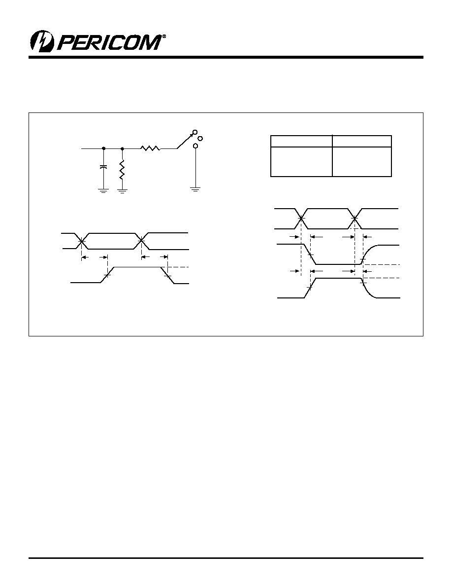
PARAMETER MEASUREMENT INFORMATION FOR A TO B PORT
V
CCA
=2.7V TO 3.6V and V
CCB
= 5V ± 0.5V
Load Circuit
Voltage Waveforms
Propagation Delay Times
Voltage Waveforms
Enable and Disable Times
Notes:
A. C
L
includes probe and jig capacitance.
B. Waveform 1 is for an output with internal conditions such that the output is low except when disabled by the output control.
Waveform 2 is for an output with internal conditions such that the output is high except when disabled by the output control.
C. All input impulses are supplied by generators having the following characteristics: PRR 10 MHz, Z
O
= 50, t
R
2.5ns, t
F
2.5ns.
D. The outputs are measured one at a time with one transition per measurement.
Figure 1. Load Circuit and Voltage Waveforms
500
500
2xVCCB
Open
GND
S1
From Output
Under Test
CL = 50pF
(See Note A)
500
500
50
Input
t
PLH
t
PHL
0V
B-Port
Output
V
OH
V
OL
1.5V
1.5V
2.7V
50% VCCB
50% VCCB
t
PZL
Output
Control
0V
1.5V
50% V
CCB
1.5V
t
PLZ
t
PHZ
V
OL
V
CCB
0V
t
PZH
+0.3V
0.3V
Output
Waveform 1
S1 at 2 x V
CCB
(see Note B)
Output
Waveform 2
S1 at GND
(see Note B)
V
OH
V
OH
V
OL
2.7V
50% V
CCB
Power- Up Considerations
To avoid excessive supply current, bus contention or oscillation during power-up, the following guidelines should be followed:
1. Connect ground first before any supply voltage is applied.
2. Power up V
CCA
, which is the control side of the device.
3. Ramp OE ahead of or with V
CCA
to help prevent bus contention
4. Ramp DIR with V
CCA
if DIR high is needed (A bus to B bus). Otherwise keep DIR Low.
Test
S1
t
PLH
/t
PHL
t
PLZ
/t
PZL
t
PHZ
/t
PZH
Open
2 x V
CCB
GND
PI74LVCC3245A
8-Bit Dual Supply Bus Transceiver with
Configurable Output Voltage and 3-State Outputs
7
PS8702A 09/10/03
PARAMETER MEASUREMENT INFORMATION FOR B TO A PORT
V
CCA
=2.7V TO 3.6V and V
CCB
= 5V ± 0.5V
Load Circuit
Voltage Waveforms
Propagation Delay Times
Voltage Waveforms
Enable and Disable Times
Notes:
A. C
L
includes probe and jig capacitance.
B. Waveform 1 is for an output with internal conditions such that the output is low except when disabled by the output control.
Waveform 2 is for an output with internal conditions such that the output is high except when disabled by the output control.
C. All input impulses are supplied by generators having the following characteristics: PRR 10 MHz, Z
O
= 50, t
R
2.5ns, t
F
2.5ns.
D. The outputs are measured one at a time with one transition per measurement.
Figure 2. Load Circuit and Voltage Waveforms
500
500
6V
Open
GND
S1
From Output
Under Test
CL = 50pF
(See Note A)
500
500
50
t
PZL
Output
Control
0V
1.5V
1.5V
1.5V
t
PLZ
t
PHZ
V
OL
3V
0V
t
PZH
+0.3V
0.3V
Output
Waveform 1
S1 at 6V
(see Note B)
Output
Waveform 2
S1 at GND
(see Note B)
V
OH
V
OH
V
OL
2.7V
1.5V
Test
S1
t
PLH
/t
PHL
t
PLZ
/t
PZL
t
PHZ
/t
PZH
Open
6V
GND
B Port
Input
t
PLH
t
PHL
0V
A-Port
Output
V
OH
V
OL
50% V
CCB
50% V
CCB
V
CCB
1.5V
1.5V

PI74LVCC3245A
8-Bit Dual Supply Bus Transceiver with
Configurable Output Voltage and 3-State Outputs
8
PS8702A 09/10/03
PARAMETER MEASUREMENT INFORMATION FOR A TO B AND B TO A
V
CCA
=2.7V TO 3.6V and V
CCB
= 3.3V ± 0.3V
Load Circuit
Voltage Waveforms
Propagation Delay Times
Voltage Waveforms
Enable and Disable Times
Notes:
A. C
L
includes probe and jig capacitance.
B. Waveform 1 is for an output with internal conditions such that the output is low except when disabled by the output control.
Waveform 2 is for an output with internal conditions such that the output is high except when disabled by the output control.
C. All input impulses are supplied by generators having the following characteristics: PRR 10 MHz, Z
O
= 50, t
R
2.5ns, t
F
2.5ns.
D. The outputs are measured one at a time with one transition per measurement.
Figure 2. Load Circuit and Voltage Waveforms
500
500
6V
Open
GND
S1
From Output
Under Test
CL = 50pF
(See Note A)
Input
t
PLH
t
PHL
0V
Output
V
OH
V
OL
1.5V
1.5V
2.7V
1.5V
1.5V
t
PZL
Output
Control
0V
1.5V
1.5V
1.5V
t
PLZ
t
PHZ
V
OL
3V
0V
t
PZH
+0.3V
0.3V
Output
Waveform 1
S1 at 6V
(see Note B)
Output
Waveform 2
S1 at GND
(see Note B)
V
OH
V
OH
V
OL
2.7V
1.5V
Test
S1
t
PLH
/t
PHL
t
PLZ
/t
PZL
t
PHZ
/t
PZH
Open
6V
GND
PI74LVCC3245A
8-Bit Dual Supply Bus Transceiver with
Configurable Output Voltage and 3-State Outputs
9
PS8702A 09/10/03
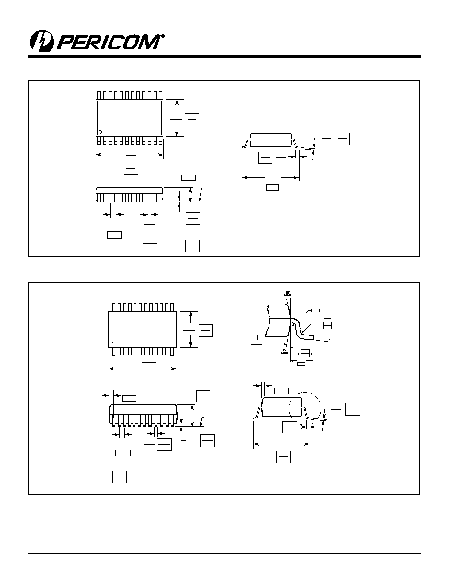
Packaging Mechanical: 24-pin TSSOP (L)
Packaging Mechanical: 24-pin QSOP (Q)
.303
.311
.047
1.20
.002
.006
SEATING
PLANE
.0256
BSC
.018
.030
.004
.008
.252
BSC
1
24
.169
.177
X.XX
X.XX
DENOTES CONTROLLING
DIMENSIONS IN MILLIMETERS
0.05
0.15
6.4
0.45
0.75
0.09
0.20
4.3
4.5
7.7
7.9
0.65
0.19
0.30
.007
.012
Max
.337
.344
.053
.069
.004
.010
SEATING
PLANE
.025
typical
.007
.010
.228
.244
1
24
.150
.157
.016
.050
X.XX
X.XX
DENOTES DIMENSIONS
IN MILLIMETERS
0.635
8.56
8.74
1.35
1.75
5.79
6.20
0.406
1.27
0.101
0.254
.008
.012
0.203
0.305
3.81
3.99
0.178
0.254
.033
0.84
0.38
.015 x 45°
Detail A
Detail A
.008
0.20
MIN.
Guage Plane
.010
0.254
.041
1.04
REF
.016
.035
0.41
0.89
0°-6°
.008
.013
0.20
0.33
PI74LVCC3245A
8-Bit Dual Supply Bus Transceiver with
Configurable Output Voltage and 3-State Outputs
10
PS8702A 09/10/03
Ordering Information
Pericom Semiconductor Corporation · 1-800-435-2336 · http://www.pericom.com
Ordering Code
Package Code
Package Desription
PI74LVCC3245AL
L
24-pin, 173-mil wide plastic TSSOP
PI74LVCC3245ALE
L
Pb-free, 24-pin, 173-mil wide plastic TSSOP
PI74LVCC3245AQ
Q
24-pin, 150-mil wide plastic QSOP
PI74LVCC3245AS
S
24-pin, 300-mil wide plastic SOIC
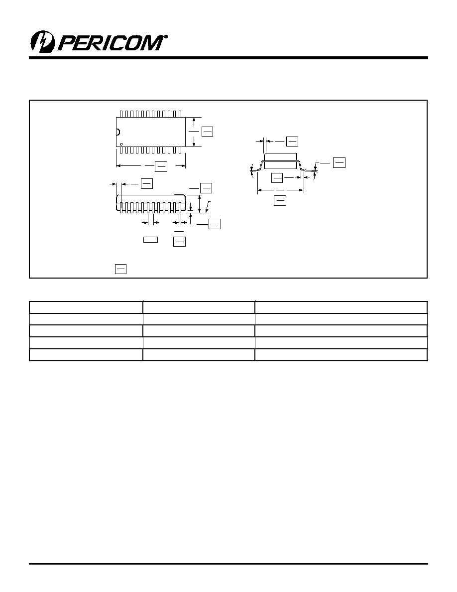
Packaging Mechanical: 24-pin SOIC (S)
SEATING
PLANE
.050
BSC
1
0-8°
.2914
.2992
X.XX
X.XX
DENOTES DIMENSIONS
IN MILLIMETERS
7.40
7.60
.5985
.6141
15.20
15.60
1.27
.0926
.1043
2.35
2.65
.394
.419
10.00
10.65
.0040
.0118
0.10
0.30
.013
.020
0.33
0.51
.010
.029
0.254
0.737
.0091
.0125
0.23
0.32
0.41
1.27
.016
.050
x 45°
24
.021
.031
0.533
0.787
Notes:
1. Thermal characteristics can be found on the company web site at http://www.pericom.com/packaging/