1
PS8437 08/24/01
Product Description
Pericom Semiconductors PI74ALVCH series of logic circuits are
produced using the Companys advanced 0.5 micron CMOS
technology, achieving industry leading speed grades.
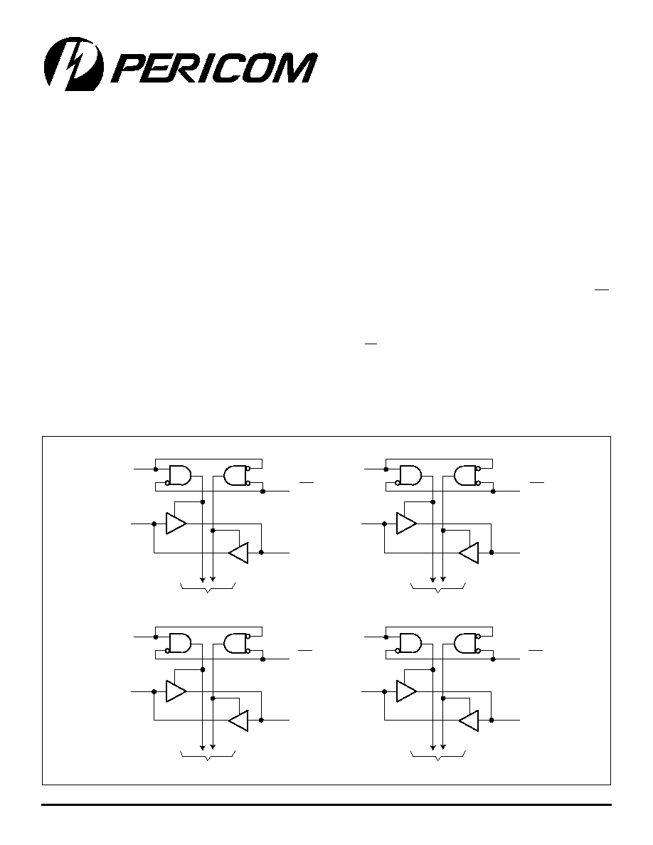
The PI74ALVCH32245 is a 32-bit bidirectional transceiver
designed for asynchronous two-way communication between
data buses. The direction control input pin (xDIR) determines
the direction of data flow through the bidirectional transceiver.
The Direction and Output Enable controls are designed to operate
this device as either four independent 8-bit transceivers, two 16-Bit
transceivers, or one 32-Bit transceiver. The output enable (OE)
input, when HIGH, disables both A and B ports by placing them in
HIGH Z condition.
To ensure the high-impedance state during power up or power
down, OE should be tied to V
CC
through a pull-up resistor; the
minimum value of the resistor is determined by the current sinking
ability of the driver.
Active bus-hold circuitry is provided to hold unused or floating
data inputs at a valid logic level.
Product Features
Ę
PI74ALVCH32245 is designed for low voltage operation
Ę
V
CC
= 2.3V to 3.6V
Ę
Typical V
OLP
(Output Ground Bounce)
< 0.8V at V
CC
= 3.3V, T
A
= 25░C
Ę
Typical V
OHV
(Output V
OH
Undershoot)
> 2.0V at V
CC
= 3.3V, T
A
= 25░C
Ę
Bus Hold retains last active bus state during 3-State,
eliminating the need for external pullup resistors
Ę
Industrial operation at 40░C to +85░C
Ę
Packages available:
96-ball, 13.5mm x 5.5mm x 1.4mm low profile fine
pitch ball grid array, LFBGA (NB)
Logic Block Diagram (Positive Logic)
1OE
1DIR
1B1
1A1
A2
A4
A5
A3
To Seven Other Channels
2OE
2DIR
2B1
2A1
E2
H4
E5
H3
To Seven Other Channels
3OE
3DIR
3B1
3A1
J2
J4
J5
J3
To Seven Other Channels
4OE
4DIR
4B1
4A1
N2
T4
N5
T3
To Seven Other Channels
12345678901234567890123456789012123456789012345678901234567890121234567890123456789012345678901212345678901234567890123456789012123456789012
12345678901234567890123456789012123456789012345678901234567890121234567890123456789012345678901212345678901234567890123456789012123456789012
3.3V, 32-Bit Bidirectional Transceiver
with 3-State Outputs
PI74ALVCH32245
2
PS8437 08/24/01
PI74ALVCH32245
3.3V, 32-Bit Bidirectional Tranceiver
with 3-State Outputs
12345678901234567890123456789012123456789012345678901234567890121234567890123456789012345678901212345678901234567890123456789012123456789012
12345678901234567890123456789012123456789012345678901234567890121234567890123456789012345678901212345678901234567890123456789012123456789012
6
2
A
1
4
A
1
6
A
1
8
A
1
2
A
2
4
A
2
6
A
2
7
A
2
2
A
3
4
A
3
6
A
3
8
A
3
2
A
4
4
A
4
6
A
4
7
A
4
5
1
A
1
3
A
1
5
A
1
7
A
1
1
A
2
3
A
2
5
A
2
8
A
2
1
A
3
3
A
3
5
A
3
7
A
3
1
A
4
3
A
4
5
A
4
8
A
4
4
E
O
1
D
N
G
V
C
C
D
N
G
D
N
G
V
C
C
D
N
G
E
O
2
E
O
3
D
N
G
V
C
C
D
N
G
D
N
G
V
C
C
D
N
G
E
O
4
3
R
I
D
1
D
N
G
V
C
C
D
N
G
D
N
G
V
C
C
D
N
G
R
I
D
2
R
I
D
3
D
N
G
V
C
C
D
N
G
D
N
G
V
C
C
D
N
G
R
I
D
4
2
1
B
1
3
B
1
5
B
1
7
B
1
1
B
2
3
B
2
5
B
2
8
B
2
1
B
3
3
B
3
5
B
3
7
B
3
1
B
4
3
B
4
5
B
4
8
B
4
1
2
B
1
4
B
1
6
B
1
8
B
1
2
B
2
4
B
2
6
B
2
7
B
2
2
B
3
4
B
3
6
B
3
8
B
3
2
B
4
4
B
4
6
B
4
7
B
4
A
B
C
D
E
F
G
H
J
K
L
M
N
P
R
T
Pin Name
Description
xOE
3-State Output Enable Inputs (Active LOW)
xDIR
Direction Control Input
xAx
Side A Inputs or 3-State Inputs
xBx
Side B Outputs or 3-State Outputs
GND
Ground
V
CC
Power
Product Pin Description
Truth Table
(1)
Notes:
1. H = High Voltage Level
L = Low Voltage Level
X = Dont Care
Z = High Impedance
s
t
u
p
n
I
)
1
(
s
t
u
p
t
u
O
)
1
(
E
O
x
R
I
D
x
L
L
A
s
u
B
o
t
a
t
a
D
B
s
u
B
L
H
B
s
u
B
o
t
a
t
a
D
A
s
u
B
H
X
Z
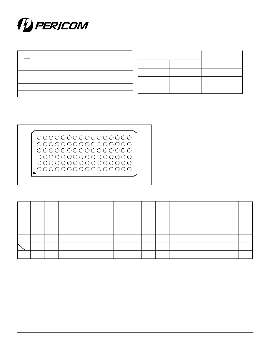
NB Package (Top View)
A B C D E F G H J K L M N P R T
6
5
4
3
2
1
Terminal Assignments

PI74ALVCH32245
3.3V, 32-Bit Bidirectional Tranceiver
with 3-State Outputs
3
PS8437 08/24/01
12345678901234567890123456789012123456789012345678901234567890121234567890123456789012345678901212345678901234567890123456789012123456789012
12345678901234567890123456789012123456789012345678901234567890121234567890123456789012345678901212345678901234567890123456789012123456789012
Note:
Stresses greater than those listed under MAXIMUM
RATINGS may cause permanent damage to the device.
This is a stress rating only and functional operation of the
device at these or any other conditions above those indi-
cated in the operational sections of this specification is not
implied. Exposure to absolute maximum rating conditions
for extended periods may affect reliability.
Recommended Operating Conditions
(1)
Maximum Ratings
(Above which the useful life may be impaired. For user guidelines, not tested.)
s
r
e
t
e
m
a
r
a
P
n
o
it
p
i
r
c
s
e
D
s
n
o
it
i
d
n
o
C
t
s
e
T
.
n
i
M
.
p
y
T
.
x
a
M
s
ti
n
U
V
C
C
e
g
a
tl
o
V
y
l
p
p
u
S
3
.
2
6
.
3
V
V
H
I
e
g
a
tl
o
V
H
G
I
H
t
u
p
n
I
V
C
C
V
7
.
2
o
t
V
3
.
2
=
7
.
1
V
C
C
V
6
.
3
o
t
V
7
.
2
=
0
.
2
V
L
I
e
g
a
tl
o
V
W
O
L
t
u
p
n
I
V
C
C
V
7
.
2
o
t
V
3
.
2
=
7
.
0
V
C
C
V
6
.
3
o
t
V
7
.
2
=
8
.
0
V
N
I
e
g
a
tl
o
V
t
u
p
n
I
0
V
C
C
V
T
U
O
e
g
a
tl
o
V
t
u
p
t
u
O
0
V
C
C
I
H
O
t
u
p
t
u
O
H
G
I
H
t
n
e
rr
u
C
V
C
C
V
3
.
2
= 2
1
A
m
V
C
C
V
7
.
2
= 2
1
V
C
C
V
0
.
3
= 4
2
I
L
O
t
u
p
t
u
O
W
O
L
t
n
e
rr
u
C
V
C
C
V
3
.
2
=
2
1
V
C
C
V
7
.
2
=
2
1
V
C
C
V
0
.
3
=
4
2
/t
V
e
t
a
R
ll
a
F
r
o
e
si
R
n
o
it
i
s
n
a
r
T
t
u
p
n
I
0
0
1
V
/
s
n
T
A
e
r
u
t
a
r
e
p
m
e
T
ri
A
-
e
e
r
F
g
n
it
a
r
e
p
O
0
4
5
8
C
░
Supply Voltage Range,V
CC ...............................................................
0.5V to 4.6V
Input Voltage Range, V
I
: Except I/O ports
(1) ..............................
0.5V to 4.6V
I/O ports
(1,2) ...........................
0.5V to V
CC
+ 0.5V
Output Voltage Range, V
O (1,2) ............................................
0.5V to V
CC
+0.5V
Input Clamp Current, I
IK
(V
I
<0) ........................................................ 50mA
Output Clamp Current, I
OK
(V
O
<0) .................................................. 50mA
Continuous Output Current, I
O ...................................................................
▒50mA
Continuous Current through each V
CC
or GND ............................... ▒100mA
Package Thermal Impedance,
JA(3) .............................................................
40║C/W
Storage Temperature Range, T
STG ...............................................
65║C to 150║C
Note:
1. The input negative voltage and output voltage ratings may be exceeded
if the input and output current ratings are observed.
2. This value is limited to 4.6V maximum.
3. The package thermal impedance is calculated in accordance with JESD 51.
Note 1: All unused inputs must be held at V
CC
or GND to ensure proper device operation
4
PS8437 08/24/01
PI74ALVCH32245
3.3V, 32-Bit Bidirectional Tranceiver
with 3-State Outputs
12345678901234567890123456789012123456789012345678901234567890121234567890123456789012345678901212345678901234567890123456789012123456789012
12345678901234567890123456789012123456789012345678901234567890121234567890123456789012345678901212345678901234567890123456789012123456789012
s
r
e
t
e
m
a
r
a
P
n
o
it
p
i
r
c
s
e
D
s
n
o
it
i
d
n
o
C
t
s
e
T
)
1
(
.
n
i
M
.
p
y
T
)
2
(
.
x
a
M
s
ti
n
U
V
H
O
e
g
a
tl
o
V
H
G
I
H
t
u
p
t
u
O
I
H
O
0
0
1
-
=
Ą
V
,
A
C
C
.
x
a
M
o
t
.
n
i
M
=
V
-
C
C
2
.
0
V
V
H
I
I
,
V
7
.
1
=
H
O
A
m
6
-
=
,
V
=
C
C
V
3
.
2
0
.
2
V
H
I
I
,
V
7
.
1
=
H
O
A
m
2
1
-
=
,
V
=
C
C
V
3
.
2
7
.
1
V
H
I
I
,
V
0
.
2
=
H
O
A
m
2
1
-
=
,
V
=
C
C
V
7
.
2
2
.
2
V
H
I
I
,
V
0
.
2
=
H
O
A
m
2
1
-
=
,
V
C
C
V
0
.
3
=
4
.
2
V
H
I
I
,
V
0
.
2
=
H
O
A
m
4
2
-
=
,
V
C
C
V
0
.
3
=
0
.
2
V
L
O
e
g
a
tl
o
V
W
O
L
t
u
p
t
u
O
I
L
O
0
0
1
-
=
Ą
V
,
A
L
I
.
x
a
M
o
t
.
n
i
M
=
2
.
0
V
L
I
I
,
V
7
.
0
=
L
O
A
m
6
=
,
V
=
C
C
V
3
.
2
4
.
0
V
L
I
I
,
V
7
.
0
=
L
O
A
m
2
1
=
,
V
=
C
C
V
3
.
2
7
.
0
V
L
I
I
,
V
8
.
0
=
L
O
A
m
2
1
=
,
V
=
C
C
V
7
.
2
4
.
0
V
L
I
I
,
V
8
.
0
=
L
O
A
m
4
2
=
,
V
C
C
V
0
.
3
=
5
5
.
0
I
N
I
t
n
e
rr
u
C
t
u
p
n
I
V
N
I
V
=
C
C
V
,
D
N
G
r
o
C
C
V
6
.
3
=
5
▒
Ą
A
I
N
I
(
HOLD
)
d
l
o
H
t
u
p
n
I
t
n
e
rr
u
C
V
N
I
V
,
V
7
.
0
=
C
C
V
3
.
2
=
5
4
V
N
I
V
,
V
7
.
1
=
C
C
V
3
.
2
=
5
4
V
N
I
V
,
V
8
.
0
=
C
C
V
0
.
3
=
5
7
V
N
I
V
,
V
0
.
2
=
C
C
V
0
.
3
=
5
7
V
N
I
0
=
o
t
V
,
V
6
.
3
C
C
V
6
.
3
=
)
3
(
0
0
5
▒
I
Z
O
)
st
u
p
t
u
O
e
t
a
t
S
-
3
(
t
n
e
rr
u
C
t
u
p
t
u
O
V
T
U
O
V
=
C
C
r
o
,
D
N
G
V
C
C
V
6
.
3
=
0
1
▒
I
C
C
t
n
e
rr
u
C
y
l
p
p
u
S
V
C
C
=
V
6
.
3
I
,
T
U
O
0
=
Ą
,
A
V
N
I
V
r
o
D
N
G
=
C
C
0
4
I
C
C
t
u
p
n
I
r
e
p
t
n
e
rr
u
C
y
l
p
p
u
S
H
G
I
H
L
T
T
@
V
C
C
V
0
.
3
=
o
t
6
.
3 V
V
t
a
t
u
p
n
I
e
n
O
C
C
-
V
6
.
0
V
t
a
st
u
p
n
I
r
e
h
t
O
C
C
D
N
G
r
o
0
5
7
C
I
st
u
p
n
I
l
o
rt
n
o
C
V
N
I
V
=
C
C
V
,
D
N
G
r
o
C
C
V
3
.
3
=
4
F
p
C
O
I
st
r
o
P
B
r
o
A
V
O
V
=
C
C
V
,
D
N
G
r
o
C
C
V
3
.
3
=
8
Notes:
1. For Min. or Max conditions, use appropriate value specified under Electrical Characteristics for the applicable device type.
2. Typical values are at V
CC
= 3.3V, +25░C ambient and maximum loading.
3. This is the bushold maximum dynamic current. It is the mimum overdrive current necessary to switch the input from one
state to another.
DC Electrical Characteristics
(Over the Operating Range, T
A
= 40░C to +85░C, V
CC
= 3.3V ▒10%)
PI74ALVCH32245
3.3V, 32-Bit Bidirectional Tranceiver
with 3-State Outputs
5
PS8437 08/24/01
12345678901234567890123456789012123456789012345678901234567890121234567890123456789012345678901212345678901234567890123456789012123456789012
12345678901234567890123456789012123456789012345678901234567890121234567890123456789012345678901212345678901234567890123456789012123456789012
s
r
e
t
e
m
a
r
a
P
)
T
U
P
N
I
(
m
o
r
F
)
T
U
P
T
U
O
(
o
T
V
C
C
V
2
.
0
▒
V
5
.
2
=
V
C
C
V
7
.
2
=
V
C
C
V
3
.
0
▒
V
3
.
3
=
s
ti
n
U
.
n
i
M
)
2
(
.
x
a
M
.
n
i
M
)
2
(
.
x
a
M
.
n
i
M
)
2
(
.
x
a
M
t
D
P
B
r
o
A
A
r
o
B
0
.
1
7
.
3
6
.
3
0
.
1
0
.
3
s
n
t
N
E
E
O
A
r
o
B
0
.
1
7
.
5
4
.
5
0
.
1
4
.
4
t
S
I
D
E
O
A
r
o
B
5
.
1
2
.
5
6
.
4
0
.
1
1
.
4
Switching Characteristics over Operating Range
(1)
Operating Characteristics, T
A
= 25║C
r
e
t
e
m
a
r
a
P
s
n
o
it
i
d
n
o
C
t
s
e
T
V
C
C
V
2
.
0
▒
V
5
.
2
=
V
C
C
V
3
.
0
▒
V
3
.
3
=
s
ti
n
U
l
a
c
i
p
y
T
C
D
P
n
o
it
a
p
i
s
si
D
r
e
w
o
P
e
c
n
a
ti
c
a
p
a
C
d
el
b
a
n
E
st
u
p
t
u
O
C
L
,
F
p
0
5
=
z
H
M
0
1
=
f
4
4
8
5
F
p
d
el
b
a
si
D
st
u
p
t
u
O
8
0
1
Notes:
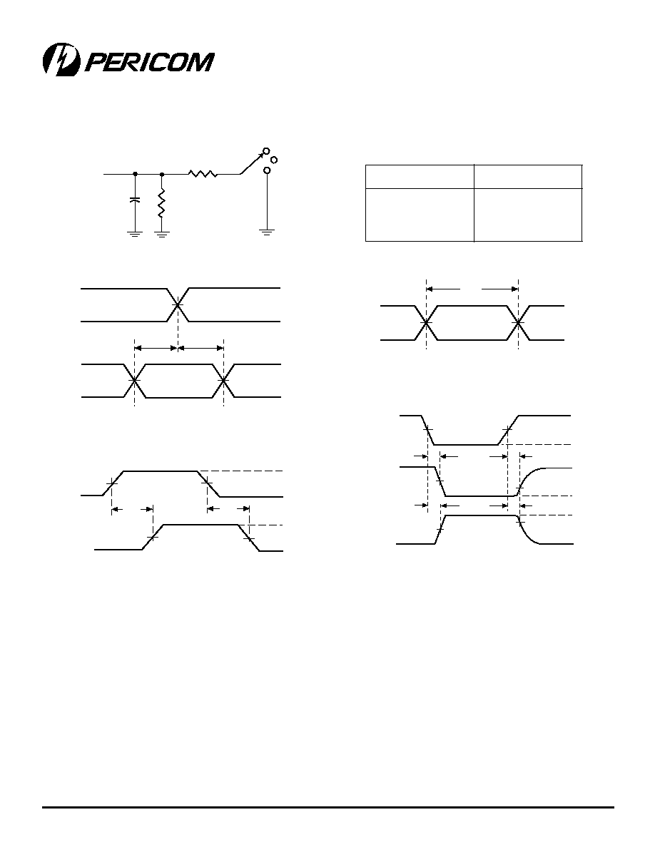
1. See test circuit and waveforms, Figures 1 and 2.
2. Minimum limits are guaranteed but not tested on Propagation Delays.

6
PS8437 08/24/01
PI74ALVCH32245
3.3V, 32-Bit Bidirectional Tranceiver
with 3-State Outputs
12345678901234567890123456789012123456789012345678901234567890121234567890123456789012345678901212345678901234567890123456789012123456789012
12345678901234567890123456789012123456789012345678901234567890121234567890123456789012345678901212345678901234567890123456789012123456789012
500
500
2 x V
CC
Open
GND
S1
From Output
Under Test
CL = 30pF
(See Note A)
t
PZL
Output
Control
(Low Level
Enabling)
0V
V
CC
/2
V
CC
/2
V
CC
/2
V
CC
/2
t
PLZ
t
PHZ
V
OL
V
CC
0V
t
PZH
+0.15V
Ł0.15V
Output
Waveform 1
S1 at 2 x V
CC
(see Note B)
Output
Waveform 2
S1 at GND
(see Note B)
V
OH
V
OH
V
OL
V
CC
Input
t
PLH
t
PHL
0V
Output
V
OH
V
OL
V
CC
/2
V
CC
/2
V
CC
/2
V
CC
VCC/2
Input
t
W
V
CC
/2
V
CC
V
CC
/2
0V
Data
Input
t
su
t
h
V
CC
/2
V
CC
V
CC
/2
0V
V
CC
0V
Timing
Input
V
CC
/2
PARAMETER MEASUREMENT INFORMATION
V
CC
= 2.5V ▒0.2V
Load Circuit
Voltage Waveforms
Setup and Hold Times
Voltage Waveforms
Propagation Delay Times
Voltage Waveforms
Enable and Disable Times
Voltage Waveforms
Pulse Duration
t
s
e
T
1
S
t
d
p
t
Z
L
P
t/
H
Z
P
t
Z
H
P
t/
H
Z
P
n
e
p
O
V
x
2
C
C
D
N
G
Notes:
A. C
L
includes probe and jig capacitance.
B. Waveform 1 is for an output with internal conditions such that the output is low except when disabled by the output control.
Waveform 2 is for an output with internal conditions such that the output is high except when disabled by the output control.
C. All input impulses are supplied by generators having the following characteristics: PRR
MHz, Z
O
= 50
, t
R
2.0ns, t
F
2.0ns.
D. The outputs are measured one at a time with one transition per measurement.
E. t
PLZ
and t
PHZ
are the same as t
dis
F. t
PZL
and t
PZH
are the same as t
en
G. t
PLH
and t
PHL
are the same as t
pd
Figure 1. Load Circuit and Voltage Waveforms
PI74ALVCH32245
3.3V, 32-Bit Bidirectional Tranceiver
with 3-State Outputs
7
PS8437 08/24/01
12345678901234567890123456789012123456789012345678901234567890121234567890123456789012345678901212345678901234567890123456789012123456789012
12345678901234567890123456789012123456789012345678901234567890121234567890123456789012345678901212345678901234567890123456789012123456789012
Pericom Semiconductor Corporation
2380 Bering Drive Ę San Jose, CA 95131 Ę 1-800-435-2336 Ę Fax (408) 435-1100 Ę http://www.pericom.com
PARAMETER MEASUREMENT INFORMATION
V
CC
= 2.7V and 3.3V ▒0.3V
Load Circuit
Voltage Waveforms
Setup and Hold Times
Voltage Waveforms
Propagation Delay Times
Voltage Waveforms
Enable and Disable Times
Voltage Waveforms
Pulse Duration
Notes:
A. C
L
includes probe and jig capacitance.
B. Waveform 1 is for an output with internal conditions such that the output is low except when disabled by the output control.
Waveform 2 is for an output with internal conditions such that the output is high except when disabled by the output control.
C. All input impulses are supplied by generators having the following characteristics: PRR
MHz, Z
O
= 50
, t
R
2.5ns, t
F
2.5ns.
D. The outputs are measured one at a time with one transition per measurement.
E. t
PLZ
and t
PHZ
are the same as t
dis
F. t
PZL
and t
PZH
are the same as t
en
G. t
PLH
and t
PHL
are the same as t
pd
Figure 2. Load Circuit and Voltage Waveforms
500
500
6V
Open
GND
S1
From Output
Under Test
CL = 50pF
(See Note A)
Data
Input
t
su
t
h
1.5V
2.7V
1.5V
0V
2.7V
0V
Timing
Input
1.5V
Input
t
PLH
t
PHL
0V
Output
V
OH
V
OL
1.5V
1.5V
1.5V
1.5V
2.7V
Input
t
W
1.5V
2.7V
1.5V
0V
t
PZL
Output
Control
(Low Level
Enabling)
0V
1.5V
1.5V
1.5V
1.5V
t
PLZ
t
PHZ
V
OL
3V
0V
t
PZH
+0.3V
Ł0.3V
Output
Waveform 1
S1 at 6V
(see Note B)
Output
Waveform 2
S1 at GND
(see Note B)
V
OH
V
OH
V
OL
2.7V
t
s
e
T
1
S
t
d
p
t
Z
L
P
t/
H
Z
P
t
Z
H
P
t/
H
Z
P
n
e
p
O
V
6
D
N
G