Äîêóìåíòàöèÿ è îïèñàíèÿ www.docs.chipfind.ru
1
PS8734A 09/02/04
Product Features
· 14.318 MHz Crystal Input
· Selectable of 100, 133, 166, 200, 266, 333, and 400MHz CPU
Output Frequencies
· SMBus: Power Management Control
· Spread Spectrum support (-0.5% down spread)
· Packaging (Pb-free & Green available):
-56-Pin SSOP (V)
-56-Pin TSSOP (A)
Output Features
· Two Pairs of Differential CPU Clocks
· One selectable of CPU/SRC Clock
· Six Pairs of SRC Clocks
· Nine PCI Clocks
· One 48 MHz USB clock
· One REF clock
· One 96 MHz Differential clock
Product Description
PI6C410 is a high-speed, low-noise clock generator designed to
work with Intel Desktop PCI-Express Chipset.
Spread Spectrum PLL based clock generator reduce EMI emis-
sion and support a wide range of frequencies.
Jitter Performance
· < 85ps Cycle to Cycle CPU clock jitter
· < 350ps Cycle to Cycle 48MHz clock jitter
· < 500ps Cycle to Cycle PCI clock jitter
· < 125ps Cycle to Cycle SRC clock jitter
· < 1000ps Cycle to Cycle REF clock jitter
Skew Performance
· < 100ps Output to output CPU clock skew
· < 500ps Output to output PCI clock skew
· < 250ps Output to output SRC clock skew
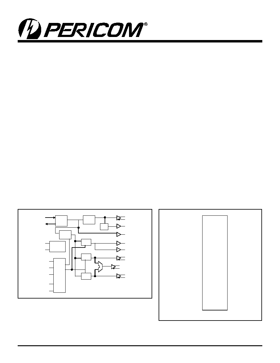
Logic Block Diagram
Pin Description
PI6C410
Clock Generator for Intel PCI-Express Desktop Chipset
Div
Div
PLL 1
XTAL
OSC
C
O
N
T
R
O
L
SMBus
Logic
REF
DOT_96
DOT 96#
USB_48
PCI [0:5]
PCIF[0:2]
SRC [1:6]
SRC [1:6]#
CPU[0:1]
CPU[0:1]#
XTAL_IN
XTAL_OUT
SDA
SCL
FS_A
FS_B / TEST_MODE
VTT_PWRGD#
/ PWRDWN
CPU2_ITP / SRC7
CPU2_ITP# / SRC7#
Div
PLL 2
FS_C / TEST_SEL
/2
PCIF_0 / ITP_EN
PCI_2
PCI_1
PCI_0
FS_C / TEST_SEL
REF
VSS_REF
XTAL_IN
XTAL_OUT
VDD_REF
SDA
SCL
VSS_CPU
CPU_0
CPU_0#
VDD_CPU
CPU_1
CPU_1#
IREF
VSS_A
VDD_A
CPU2_ITP / SRC7
CPU2_ITP# / SRC7#
VDD_SRC
SRC_6
SRC_6#
SRC_5
SRC_5#
VSS_SRC
VDD_PCI
VSS_PCI
PCI_3
PCI_4
PCI_5
VSS_PCI
VDD_PCI
PCIF_0 / ITP_EN
PCIF_1
PCIF_2
VDD_48
USB_48
VSS_48
DOT_96
DOT_96#
FS_B / TEST_MODE
VTT_PWRGD# / PWRDWN
FS_A
SRC_1
SRC_1#
VDD_SRC
SRC_2
SRC_2#
SRC_3
SRC_3#
SRC_4
SRC_4#
VDD_SRC
1
2
3
4
5
6
7
8
9
10
11
12
13
14
15
16
17
18
19
20
21
22
23
24
25
26
27
28
56
55
54
53
52
51
50
49
48
47
46
45
44
43
42
41
40
39
38
37
36
35
34
33
32
31
30
29

2
PS8734A 09/02/04
PI6C410
Clock Generator for Intel
PCI-Express Desktop Chipset
Pin Description
Pin Name
Type
Pin No
Descriptions
REF
Output
52
3.3V 14.31818MHz output
XTAL_IN
Input
50
14.31818MHz crystal input
XTAL_OUT
Output
49
14.31818MHz crystal output
CPU[0:1] & CPU[0:1]#
Output
40, 41, 43, 44
Differential CPU outputs
SRC[1:6] & SRC[1:6]#
Output
19, 20, 22, 23,
24, 25, 26, 27,
30, 31, 32, 33
Differential Serial Reference Clock outputs
CPU2_ITP / SRC_7 &
CPU2_ITP# / SRC_7#
Output
35, 36
Selectable Differential CPU or SRC clock output
ITP_EN = 0 @ Vtt_Pwrgd# assertion = SRC
ITP_EN = 1 @ Vtt_Pwrgd# assertion = CPU
PCIF_0 / ITP_EN
Input / Output
8
33MHz clock output / CPU2 select when HIGH
PCIF[1:2]
Output
9, 10
33MHz clocks outputs (free running)
PCI[0:5]
Output
3, 4, 5, 54, 55,
56
33MHz clocks outputs
USB_48
Output
12
48MHz clock output
DOT_96 & DOT_96#
Output
14, 15
96MHz differential clock output
FS_A
Input
18
3.3V LVTTL inputs for CPU frequency selection
FS_B / TEST_MODE
Input
16
3.3V LVTTL inputs for CPU frequency selection / Test Mode
select: 0 = HiZ, 1 = Ref/N
FS_C / TEST_SEL
Input
53
3.3V LVTTL inputs for CPU frequency selection / Test Mode
select if pulled to 3.3V when Vtt_Pwrgd# is asserted LOW
IREF
Input
39
External resistor connection for internal current reference
VTT_PWRGD# /
PWRDWN
Input
17
3.3V LVTTL Level sensitive strobe used to determine to latch
the FS_A, FS_B/TEST_MODE, FS_C/TEST_SEL and PCIF0/
ITP_EN inputs (active low) / 3.3V LVTTL active high input for
Power Down operation.
SDA
I/O
47
SMBus compatible SDATA
SCL
Input
46
SMBus compatible SCLOCK
VDD_PCI
Power
1, 7
3.3V Power Supply for Outputs
VDD_48
Power
11
3.3V Power Supply for Outputs
VDD_SRC
Power
21, 28, 34
3.3V Power Supply for Outputs
VDD_CPU
Power
42
3.3V Power Supply for Outputs
VDD_REF
Power
48
3.3V Power Supply for Outputs
VSS_PCI
Ground
2, 6
Ground for Outputs
VSS_48
Ground
13
Ground for Outputs
VSS_SRC
Ground
29
Ground for Outputs
VSS_CPU
Ground
45
Ground for Outputs
VSS_REF
Ground
51
Ground for Outputs
VDD_A
Power
37
3.3V Power Supply for PLL
VSS_A
Ground
38
Ground for PLL
3
PS8734A 09/02/04
PI6C410
Clock Generator for Intel
PCI-Express Desktop Chipset
Functionality
Frequency Selection
FS_C
FS_B
FS_A
CPU
SRC
PCIF / PCI
REF
DOT_96
USB_48
Note
1
0
1
100MHz
100MHz
33MHz
14.318MHz
96MHz
48MHz
1
0
0
1
133MHz
100MHz
33MHz
14.318MHz
96MHz
48MHz
1
0
1
1
166MHz
100MHz
33MHz
14.318MHz
96MHz
48MHz
1
0
1
0
200MHz
100MHz
33MHz
14.318MHz
96MHz
48MHz
1
0
0
0
266MHz
100MHz
33MHz
14.318MHz
96MHz
48MHz
1
1
0
0
333MHz
100MHz
33MHz
14.318MHz
96MHz
48MHz
1
1
1
0
400MHz
100MHz
33MHz
14.318MHz
96MHz
48MHz
1
1
1
1
Reserved
100MHz
33MHz
14.318MHz
96MHz
48MHz
1
Notes:
1. Refer to DC Electrical Characteristics for FS_A, FS_B and FS_C (Vih_FS, Vil_FS) threshold levels
Test Mode Selection
TEST_MODE
CPU
SRC
PCIF / PCI
REF
DOT_96
USB_48
Note
1
REF/N
REF/N
REF/N
REF
REF/N
REF/N
2
0
Hi-Z
Hi-Z
Hi-Z
Hi-Z
Hi-Z
Hi-Z
2
Notes:
2. Test mode will occur where the SMBus Bit 6 of Byte 6 = 1, or FS_C/TEST_SEL is set to logic high level.
PWRDWN Functionality
PWRDWN
CPU
CPU#
SRC
SRC#
PCIF /
PCI
REF
DOT_96 DOT_96# USB_48
0
Normal
Normal
Normal
Normal
33MHz 14.318MHz
Normal
Normal
48MHz
1
Iref × 2 or
Float
Float
Iref × 2 or
Float
Float
Low
Low
Iref × 2 or
Float
Float
Low
4
PS8734A 09/02/04
PI6C410
Clock Generator for Intel
PCI-Express Desktop Chipset
Serial Data Interface (SMBus)
PI6C410 is a slave only SMBus device that supports indexed block read and indexed block write protocol using a single 7-bit ad-
dress and read/write bit as shown below.
Address Assignment
A6
A5
A4
A3
A2
A1
A0
R/W
1
1
0
1
0
0
1
1/0
Data Protocol
1 bit
7 bits
1
1
8 bits
1
8 bits
1
8 bits
1
8 bits
1
1 bit
Start
bit
Slave Addr
R/W
Ack
Register
offset
Ack
Byte
Count
= N
Ack
Data
Byte 0
Ack
...
Data
Byte N
- 1
Ack Stop
bit
Notes:
1. Register offset for indicating the starting register for indexed block write and indexed block read. Byte Count in write mode cannot be 0.
Data Byte 0: Control Register
Bit
Descriptions
Type
Power Up
Condition
Output(s) Affected
Pin
Source Pin
0
Reserved
RW
1
SRC_1 Output Enable
1 = Enabled, 0 = Disabled (Hi-Z)
RW
1 = Enabled
SRC_1
19, 20
NA
2
SRC_2 Output Enable
1 = Enabled, 0 = Disabled (Hi-Z)
RW
1 = Enabled
SRC_2
22, 23
NA
3
SRC_3 Output Enable
1 = Enabled, 0 = Disabled (Hi-Z)
RW
1 = Enabled
SRC_3
24, 25
NA
4
SRC_4 Output Enable
1 = Enabled, 0 = Disabled (Hi-Z)
RW
1 = Enabled
SRC_4
26, 27
NA
5
SRC_5 Output Enable
1 = Enabled, 0 = Disabled (Hi-Z)
RW
1 = Enabled
SRC_5
30, 31
NA
6
SRC_6 Output Enable
1 = Enabled, 0 = Disabled (Hi-Z)
RW
1 = Enabled
SRC_6
32, 33
NA
7
CPU_2 / SRC_7 Output Enable
1 = Enabled, 0 = Disabled (Hi-Z)
RW
1 = Enabled
CPU_2 / SRC_7
35, 36
NA
5
PS8734A 09/02/04
PI6C410
Clock Generator for Intel
PCI-Express Desktop Chipset
Data Byte 1: Control Register
Bit
Descriptions
Type
Power Up
Condition
Output(s) Affected
Pin
Source Pin
0
Spread Spectrum
1 = On, 0 = Off
RW
0 = Spread off
CPU[0:2], SRC[1:7],
PCI[0:5], PCIF[0:2]
3, 4, 5, 8, 9, 10,
19, 20, 22, 23,
24, 25, 26, 27,
30, 31, 32, 33,
35, 36, 40, 41,
43, 44, 54, 55,
56
NA
1
CPU_0 output enable
1 = Enabled, 0 = Disabled (Hi-Z)
RW
1 = Enabled
CPU_0, CPU_0#
43, 44
NA
2
CPU_1 output enable
1 = Enabled, 0 = Disabled (Hi-Z)
RW
1 = Enabled
CPU_1, CPU_1#
40, 41
NA
3
Reserved
RW
4
REF Output Enable
1 = Enabled, 0 = Disabled
RW
1 = Enabled
REF
52
NA
5
USB_48 Output Enable
1 = Enabled, 0 = Disabled
RW
1 = Enabled
USB_48
12
NA
6
DOT_96 Output Enable
1 = Enabled, 0 = Disabled (Hi-Z)
RW
1 = Enabled
DOT_96 & DOT96#
14, 15
NA
7
PCIF_0 Output Enable
1 = Enabled, 0 = Disabled
RW
1 = Enabled
PCIF_0
8
NA
Data Byte 2: Control Register
Bit
Descriptions
Type
Power Up
Condition
Output(s) Affected
Pin
Source Pin
0
PCIF_1 Output Enable
1 = Enabled, 0 = Disabled
RW
1 = Enabled
PCIF_1
9
NA
1
PCIF_2 Output Enable
1 = Enabled, 0 = Disabled
RW
1 = Enabled
PCIF_2
10
NA
2
PCI_0 Output Enable
1 = Enabled, 0 = Disabled
RW
1 = Enabled
PCI_0
54
NA
3
PCI_1 Output Enable
1 = Enabled, 0 = Disabled
RW
1 = Enabled
PCI_1
55
NA
4
PCI _2 Output Enable
1 = Enabled, 0 = Disabled
RW
1 = Enabled
PCI_2
56
NA
5
PCI _3 Output Enable
1 = Enabled, 0 = Disabled
RW
1 = Enabled
PCI_3
3
NA
6
PCI _4 Output Enable
1 = Enabled, 0 = Disabled
RW
1 = Enabled
PCI_4
4
NA
7
PCI _5 Output Enable
1 = Enabled, 0 = Disabled
RW
1 = Enabled
PCI_5
5
NA