Äîêóìåíòàöèÿ è îïèñàíèÿ www.docs.chipfind.ru
1
PS8746C 02/01/06
Features
· Eight Pairs of Differential Clocks
· Low skew < 50ps
· Low Cycle-to-cycle jitter < 50ps
· Output Enable for all outputs
· Outputs Tristate control via SMBus
· Power Management Control
· Programmable PLL Bandwidth
· PLL or Fanout operation
· 3.3V Operation
· Packaging (Pb-Free & Green):
-- 48-Pin SSOP (V)
-- 48-Pin TSSOP (A)
PI6C20800
Description
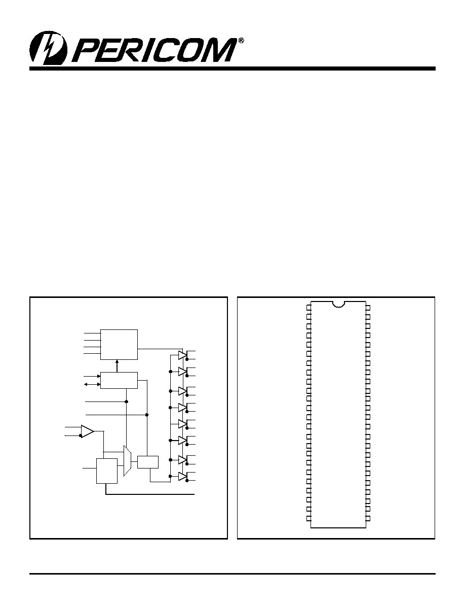
PI6C20800 is a high-speed, low-noise differential clock buffer
designed to be a companion to PI6C410B. The device distributes
the differential SRC clock from PI6C410B to eight differential
pairs of clock outputs either with or without PLL. The input
SRC clock can be divided by 2 when SRC_DIV# is LOW. The
clock outputs are controlled by input selection of SRC_STOP#,
PWRDWN# and SMBus, SCLK and SDA. When input of either
SRC_STOP# or PWRDWN# is LOW, the output clocks are
Tristated. When PWRDWN# is LOW, the SDA and SCLK inputs
must be Tristated.
Block Diagram
1:8 Clock Driver for Intel
PCI Express Chipsets
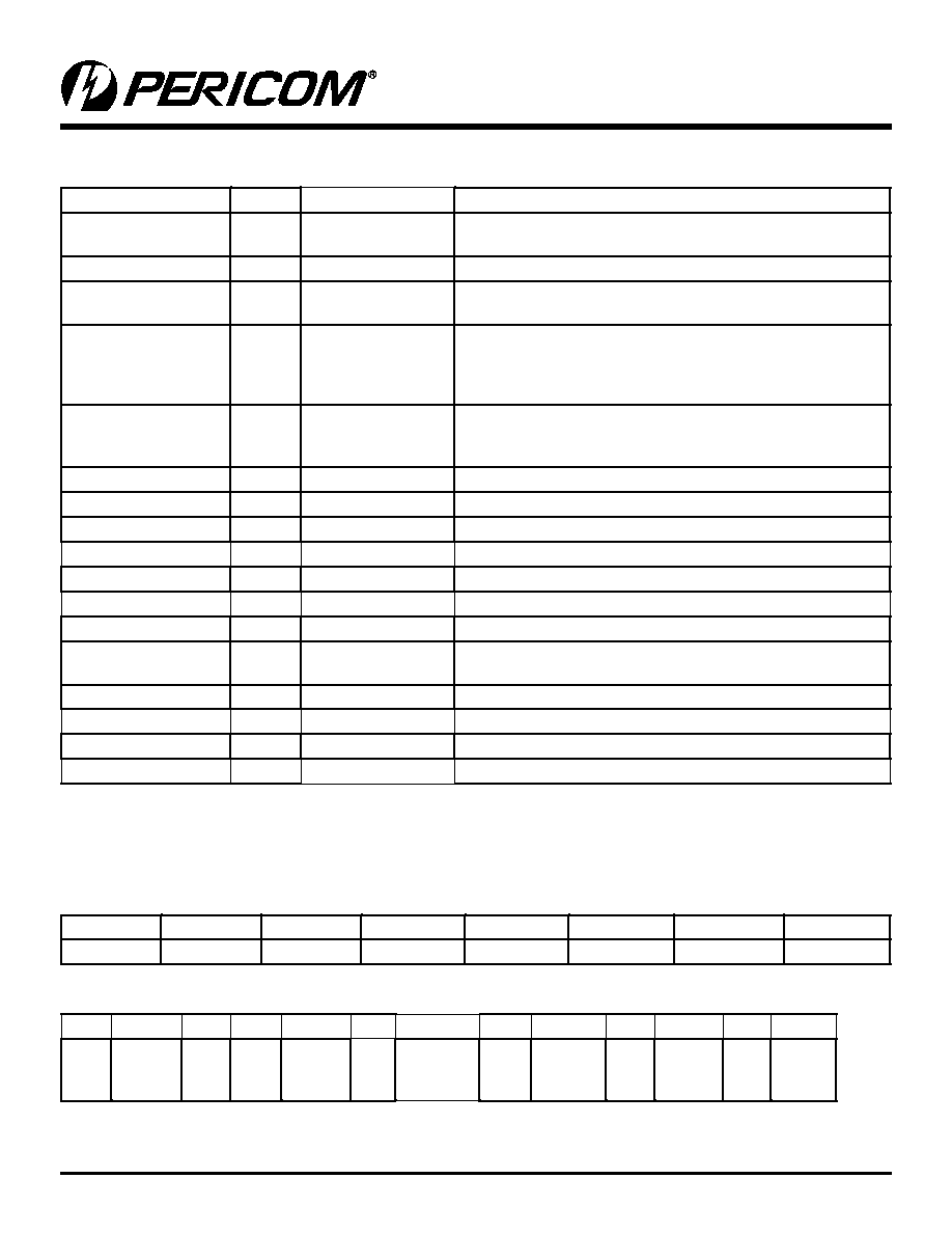
Pin Configuration
OUT0
OUT0#
OUT0
OUT1#
OUT2
OUT2#
OUT3
OUT3#
DIV
Output
Control
SMBus
Controller
PLL
PLL_BW#
SRC
SRC#
PLL/BYPASS#
SRC_DIV#
SCLK
SDA
OE_INV
OE [0:7]
SRC_STOP#
PWRDWN#
OUT4
OUT4#
OUT5
OUT5#
OUT6
OUT6#
OUT7
OUT7#
LOCK
V
DD_A
V
SS_A
I
REF
LOCK
OE_7
OE_4
OUT7
OUT7#
OE_INV
V
DD
OUT6
OUT6#
OE_6
OE_5
OUT5
OUT5#
V
SS
V
DD
OUT4
OUT4#
PLL_BW#
SRC_STOP
PWRDWN#
V
SS
48
47
46
45
44
43
42
41
40
39
38
37
36
35
34
33
32
31
30
29
28
27
26
25
1
2
3
4
5
6
7
8
9
10
11
12
13
14
15
16
17
18
19
20
21
22
23
24
SRC_DIV#
V
DD
V
SS
SRC
SRC#
OE_0
OE_3
OUT0
OUT0#
VSS
V
DD
OUT1
OUT1#
OE_1
OE_2
OUT2
OUT2#
V
SS
V
DD
OUT3
OUT3#
PLL/BYPASS#
SCLK
SDA
2
PS8746C 02/01/06
PI6C20800
1:8 Clock Driver for Intel
PCI Express Chipsets
Pin Descriptions
Pin Name
Type
Pin #
Descriptions
SRC_DIV#
Input
1
3.3V LVTTL input for selecting input frequency divide by 2,
active LOW.
SRC & SRC#
Input
4, 5
0.7V Differential SRC input from PI6C410 clock synthesizer
OE [0:7]
Input
6, 7, 14, 15, 35, 36,
43, 44
3.3V LVTTL input for enabling outputs, active HIGH.
OE_INV
Input
40
3.3V LVTTL input for inverting the OE, SRC_STOP# and
PWRDWN# pins.
When 0 = same stage
When 1 = OE[0:7], SRC_STOP#, PWRDWN# inverted.
OUT[0:7] & OUT[0:7]#
Output
8, 9, 12, 13, 16 17,
20, 21, 29, 30, 33, 34,
37, 38, 41, 42
0.7V Differential outputs
PLL/BYPASS#
Input
22
3.3V LVTTL input for selecting fan-out of PLL operation.
SCLK
Input
23
SMBus compatible SCLOCK input
SDA
I/O
24
SMBus compatible SDATA
I
REF
Input
46
External resistor connection to set the differential output current
SRC_STOP#
Input
27
3.3V LVTTL input for SRC stop, active LOW
PLL_BW#
Input
28
3.3V LVTTL input for selecting the PLL bandwidth
PWRDWN#
Input
26
3.3V LVTTL input for Power Down operation, active LOW
LOCK
Output
45
3.3V LVTTL output, transition high when PLL lock is achieved
(Latched output)
V
DD
Power
2, 11, 19, 31, 39
3.3V Power Supply for Outputs
V
SS
Ground
3, 10, 18, 25, 32
Ground for Outputs
V
SS_A
Ground
47
Ground for PLL
V
DD_A
Power
48
3.3V Power Supply for PLL
Serial Data Interface (SMBus)
PI6C20800 is a slave only SMBus device that supports indexed block read and indexed block write protocol using a single 7-bit
address and read/write bit as shown below.
Address assignment
A6
A5
A4
A3
A2
A1
A0
R/W
1
1
0
1
1
1
0
0/1
Data Protocol
(1)
1 bit
7 bits
1
1
8 bits
1
8 bits
1
8 bits
1
8 bits
1
1 bit
Start
bit
Slave
Addr
R/W
Ack
Register
offset
Ack
Byte
Count
= N
Ack
Data
Byte 0
Ack
Data
Byte N
- 1
Ack
Stop
bit
Note:
1. Register offset for indicating the starting register for indexed block write and indexed block read. Byte Count in write mode cannot be 0.
3
PS8746C 02/01/06
PI6C20800
1:8 Clock Driver for Intel
PCI Express Chipsets
Data Byte 0: Control Register
Bit
Descriptions
Type
Power Up Condition
Output(s) Affected
Pin
0
SRC_DIV#
0 = Divide by 2
1 = Normal
RW
1 = x1
OUT[0:7], OUT[0:7]#
NA
1
PLL/BYPASS#
0 = Fanout
1 = PLL
RW
1 = PLL
OUT[0:7], OUT[0:7]#
NA
2
PLL Bandwidth
0 = HIGH Bandwidth,
1 = LOW Bandwidth
RW
1 = Low
OUT[0:7], OUT[0:7]#
NA
3
TBD
NA
4
TBD
NA
5
TBD
NA
6
SRC_STOP#
0 = Driven when stopped
1 = Tristate
RW
0 = Driven when stopped
OUT[0:7], OUT[0:7]#
7
PWRDWN#
0 = Driven when stopped
1 = Tristate
RW
0 = Driven when stopped
OUT[0:7], OUT[0:7]#
NA
Data Byte 1: Control Register
Bit
Descriptions
Type
Power Up Condition
Output(s) Affected
Pin
0
OUTPUTS enable
1 = Enabled
0 = Disabled
RW
1 = Enabled
OUT0, OUT0#
NA
1
RW
1 = Enabled
OUT1, OUT1#
NA
2
RW
1 = Enabled
OUT2, OUT2#
NA
3
RW
1 = Enabled
OUT3, OUT3#
NA
4
RW
1 = Enabled
OUT4, OUT4#
NA
5
RW
1 = Enabled
OUT5, OUT5#
NA
6
RW
1 = Enabled
OUT6, OUT6#
NA
7
RW
1 = Enabled
OUT7, OUT7#
NA
4
PS8746C 02/01/06
PI6C20800
1:8 Clock Driver for Intel
PCI Express Chipsets
Data Byte 2: Control Register
Bit
Descriptions
Type
Power Up Condition
Output(s) Affected
Pin
0
Allow control of OUTPUTS with
assertion of SRC_STOP#
0 = Free running
1 = Stopped with SRC_Stop#
RW
0 = Free running
OUT0, OUT0#
NA
1
RW
0 = Free running
OUT1, OUT1#
NA
2
RW
0 = Free running
OUT2, OUT2#
NA
3
RW
0 = Free running
OUT3, OUT3#
NA
4
RW
0 = Free running
OUT4, OUT4#
NA
5
RW
0 = Free running
OUT5, OUT5#
NA
6
RW
0 = Free running
OUT6, OUT6#
NA
7
RW
0 = Free running
OUT7, OUT7#
NA
Data Byte 3: Control Register
Bit
Descriptions
Type
Power Up Condition
Output(s) Affected
Pin
0
TBD
RW
1
RW
2
RW
3
RW
4
RW
5
RW
6
RW
7
RW
Data Byte 4: Pericom ID Register
Bit
Descriptions
Type
Power Up Condition
Output(s) Affected
Pin
0
Pericom ID
R
0
NA
NA
1
R
0
NA
NA
2
R
0
NA
NA
3
R
0
NA
NA
4
R
0
NA
NA
5
R
1
NA
NA
6
R
0
NA
NA
7
R
0
NA
NA
5
PS8746C 02/01/06
PI6C20800
1:8 Clock Driver for Intel
PCI Express Chipsets
Functionality
PWRDWN#
OUT
OUT#
SRC_Stop#
OUT
OUT#
1
Normal
Normal
1
Normal
Normal
0
I
REF
× 2 or Float
LOW
0
I
REF
× 6 or Float
LOW
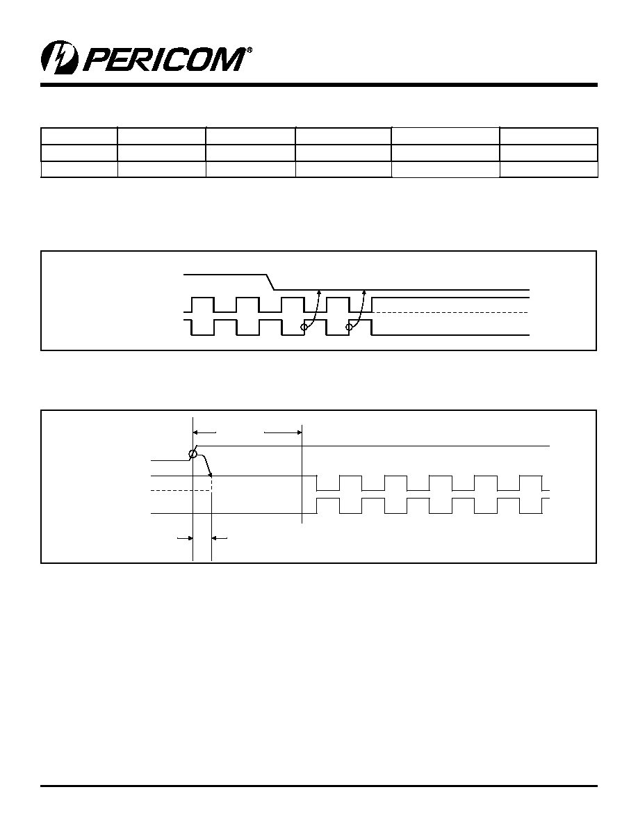
Power Down (PWRDWN# assertion)
Figure 1. Power down sequence
Power Down (PWRDWN# De-assertion)
Figure 2. Power down de-assert sequence
PWRDWN#
OUT#
OUT
PWRDWN#
OUT
OUT#
Tdrive_PwrDwn#
<300us, >200mV
Tstable
<1ms