Äîêóìåíòàöèÿ è îïèñàíèÿ www.docs.chipfind.ru
1
PS8468 05/03/00
Product Features
·
High-speed, to 140 MHz
·
Low-noise non-inverting 1-18 buffer
·
Supports up to four SDRAM DIMMs
·
Low skew (< 250ps) between any two output clocks
·
I
2
C Serial Configuration interface
·
Multiple V
DD
, V
SS
pins for noise reduction
·
3.3V power supply voltage
·
Separate Hi-Z pin for testing
·
48-pin SSOP package (V)
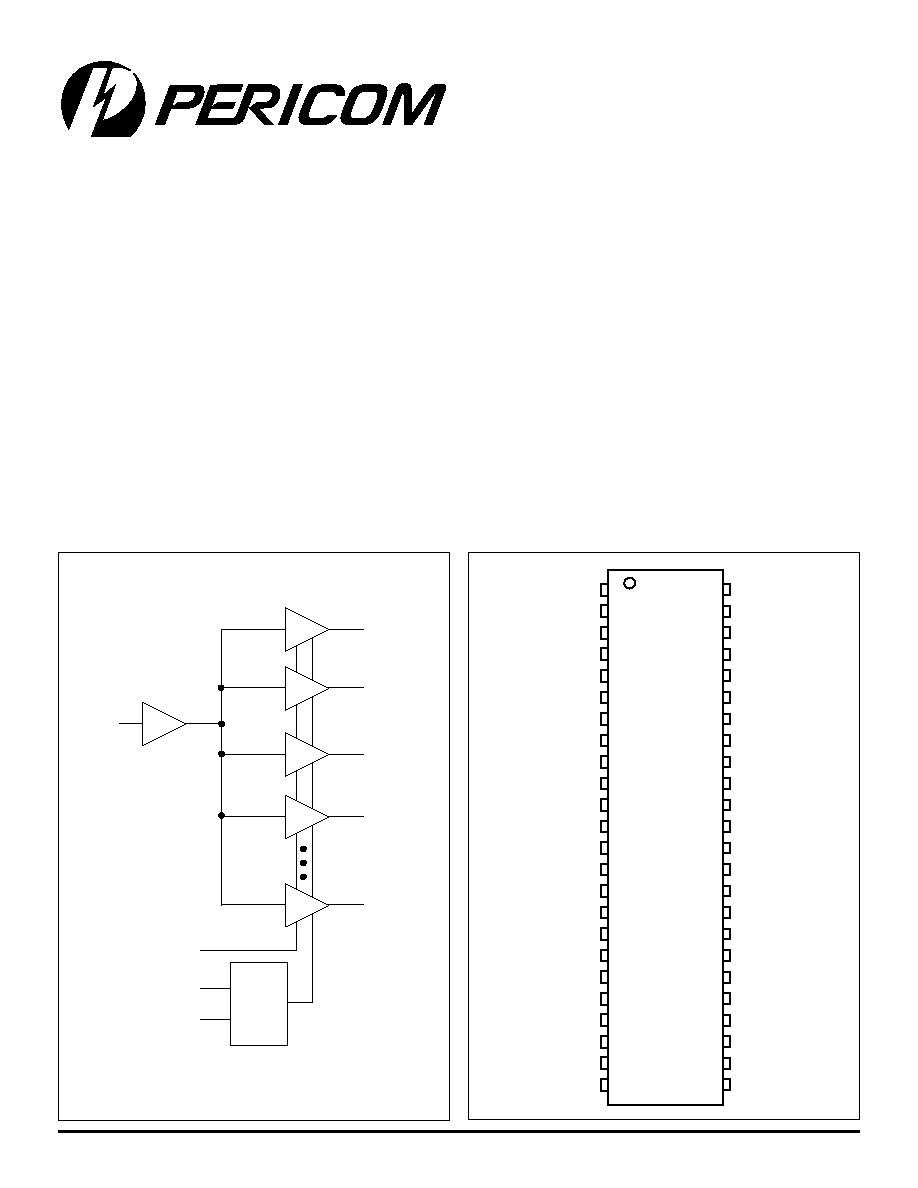
Logic Block Diagram
Description
The PI6C180B, a high-speed low-noise 1-18 noninverting buffer
designed for 140 MHz SDRAM clock buffer applications.
At power up all SDRAM output are enabled and active. The I
2
C
Serial control may be used to individually activate/deactivate any
of the 18 output drivers.
The output enable (OE) pin may be pulled low to put all outputs in a
Hi-Z state.
Note:
Purchase of I
2
C components from Pericom conveys a license to
use them in an I
2
C system as defined by Philips.
SDRAM17
SDRAM2
SDRAM1
SDRAM0
BUF_IN
OE
SDATA
SCLOCK
SDRAM3
I2C
I/O
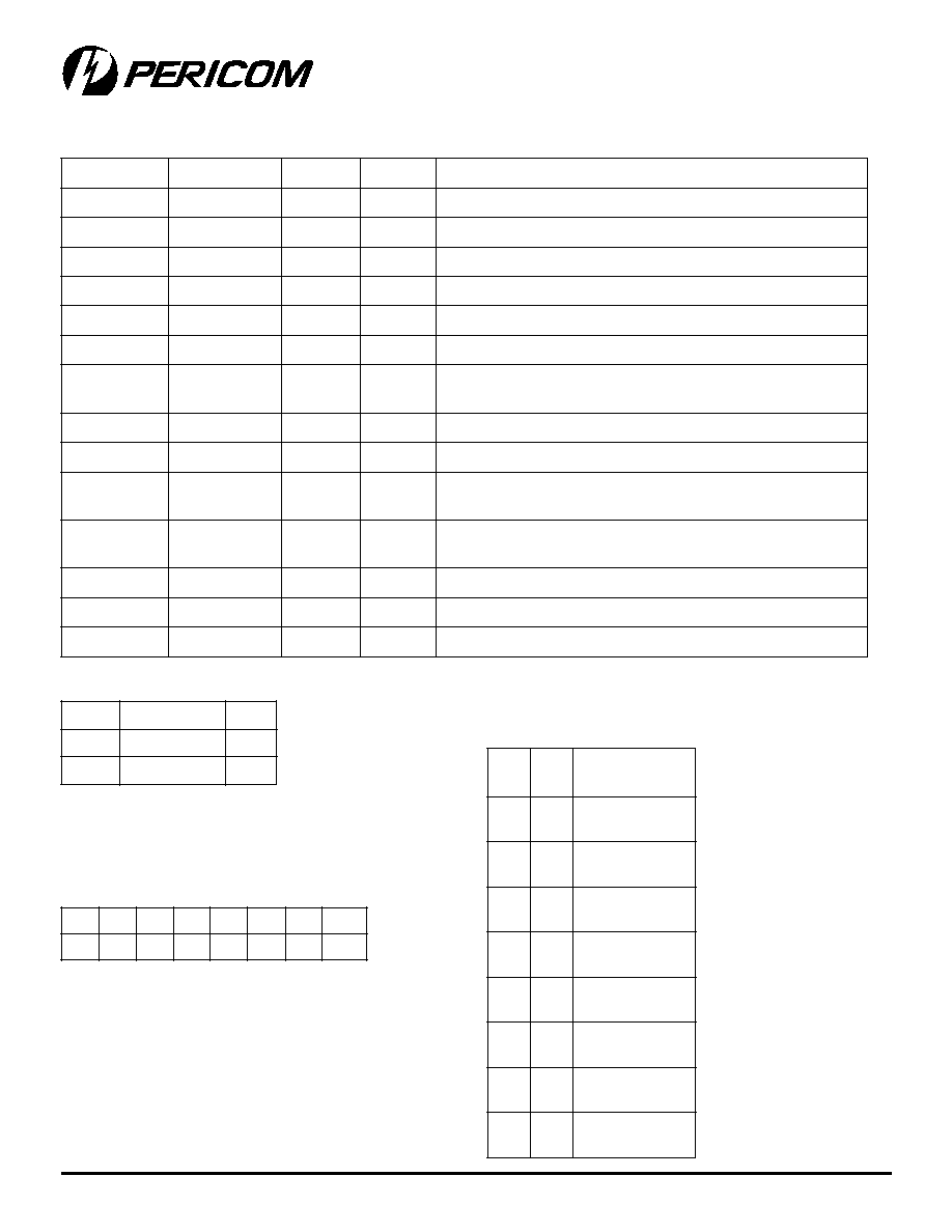
Product Pin Configuration
12345678901234567890123456789012123456789012345678901234567890121234567890123456789012345678901212345678901234567890123456789012123456789012
12345678901234567890123456789012123456789012345678901234567890121234567890123456789012345678901212345678901234567890123456789012123456789012
12345678901234567890123456789012123456789012345678901234567890121234567890123456789012345678901212345678901234567890123456789012123456789012
PI6C180B
Precision 1-18 Clock Buffer
NC
1
NC
2
V
DD0
3
SDRAM0
4
SDRAM1
5
V
SS0
6
V
DD1
7
SDRAM2
8
SDRAM3
9
V
SS1
10
BUF_IN
11
V
DD2
12
SDRAM4
13
SDRAM5
14
V
SS2
15
V
DD3
16
SDRAM6
17
SDRAM7
18
V
SS3
19
V
DD4
20
SDRAM16
21
V
SS4
22
V
DDIIC
23
SDATA
24
NC
NC
V
DD9
SDRAM15
SDRAM14
V
SS9
V
DD8
SDRAM13
SDRAM12
48
V
SS8
47
OE
46
V
DD7
45
SDRAM11
44
SDRAM10
43
V
SS7
42
V
DD6
41
SDRAM9
40
SDRAM8
39
V
SS6
38
V
DD5
37
SDRAM17
36
V
SS5
35
V
SS
IIC
34
SCLOCK
33
32
31
30
29
28
27
26
25
48-Pin
V
2
PS8468 05/03/00
12345678901234567890123456789012123456789012345678901234567890121234567890123456789012345678901212345678901234567890123456789012123456789012
12345678901234567890123456789012123456789012345678901234567890121234567890123456789012345678901212345678901234567890123456789012123456789012
PI6C180B
Precision 1-18 Clock Buffer
n
i
P
l
o
b
m
y
S
e
p
y
T
y
t
Q
n
o
it
p
i
r
c
s
e
D
9
,
8
,
5
,
4
]
3
-
0
[
M
A
R
D
S
O
4
t
u
p
t
u
o
k
c
o
l
c
0
e
t
y
B
M
A
R
D
S
8
1
,
7
1
,
4
1
,
3
1
]
7
-
4
[
M
A
R
D
S
O
4
t
u
p
t
u
o
k
c
o
l
c
1
e
t
y
B
M
A
R
D
S
6
3
,
5
3
,
2
3
,
1
3
]
1
1
-
8
[
M
A
R
D
S
O
4
t
u
p
t
u
o
k
c
o
l
c
2
e
t
y
B
M
A
R
D
S
5
4
,
4
4
,
1
4
,
0
4
]
5
1
-
2
1
[
M
A
R
D
S
O
4
t
u
p
t
u
o
k
c
o
l
c
3
e
t
y
B
M
A
R
D
S
8
2
,
1
2
]
7
1
-
6
1
[
M
A
R
D
S
O
4
k
c
a
b
d
e
e
f
r
o
f
el
b
a
s
u
st
u
p
t
u
o
k
c
o
l
c
M
A
R
D
S
1
1
N
I
_
F
U
B
I
1
r
e
ff
u
b
8
1
-
1
r
o
f
t
u
p
n
I
8
3
E
O
I
1
k
0
0
1
>
a
s
a
H
.
W
O
L
d
l
e
h
n
e
h
w
st
u
p
t
u
o
ll
a
Z
-i
H
l
a
n
r
e
t
n
i
r
o
t
si
s
e
r
p
u
-l
l
u
p
4
2
A
T
A
D
S
O
/I
1
I
r
o
f
n
i
p
a
t
a
D
2
k
0
0
1
>
a
s
a
H
.y
rt
i
u
c
ri
c
C
r
o
t
si
s
e
r
p
u
-l
l
u
p
l
a
n
r
e
t
n
i
5
2
K
C
O
L
C
S
O
/I
1
I
n
i
p
k
c
o
l
C
2
k
0
0
1
>
a
s
a
H
.y
rt
i
u
c
ri
c
C
r
o
t
si
s
e
r
p
u
-l
l
u
p
l
a
n
r
e
t
n
i
,
0
2
,
6
1
,
2
1
,
7
,
3
6
4
,
2
4
,
7
3
,
3
3
,
9
2
V
9
-
0
[
D
D
]
r
e
w
o
P
0
1
s
r
e
ff
u
b
M
A
R
D
S
r
o
f
y
l
p
p
u
s
r
e
w
o
p
V
3
.
3
,
2
2
,
9
1
,
5
1
,
0
1
,
6
3
4
,
9
3
,
4
3
,
0
3
,
7
2
V
9
-
0
[
S
S
]
d
n
u
o
r
G
0
1
s
r
e
ff
u
b
M
A
R
D
S
r
o
f
d
n
u
o
r
G
3
2
V
C
II
D
D
r
e
w
o
P
1
I
r
o
f
y
l
p
p
u
s
r
e
w
o
p
V
3
.
3
2
y
rt
i
u
c
ri
c
C
6
2
V
C
II
S
S
d
n
u
o
r
G
1
I
r
o
f
d
n
u
o
r
G
2
y
rt
i
u
c
ri
c
C
8
4
,
7
4
,
2
,
1
C
N
d
e
v
r
e
s
e
R
4
st
c
e
n
n
o
c
o
N
.
n
o
it
a
ci
fi
d
o
m
e
r
u
t
u
f
r
o
f
d
e
v
r
e
s
e
R
Product Pin Description
OE Functionality
PI6C180 I
2
C Address Assignment
Notes:
1. Used for test purposes only
2. Buffers are non-inverting
PI6C180B Serial Configuration Map
Byte0: SDRAM Active/Inactive Register
(1 = enable, 0 = disable)
Note:
Inactive means outputs are
held LOW and are disabled
from switching.
E
O
]
7
1
-
0
[
M
A
R
D
S
e
t
o
N
0
Z
-i
H
1
1
N
I
_
F
U
B
2
6
A
5
A
4
A
3
A
2
A
1
A
0
A
W
/
R
1
1
0
1
0
0
1
0
ti
B
#
n
i
P
n
o
it
p
i
r
c
s
e
D
7
ti
B
8
1
7
M
A
R
D
S
)
e
v
it
c
a
n
I/
e
v
it
c
A
(
6
ti
B
7
1
6
M
A
R
D
S
)
e
v
it
c
a
n
I/
e
v
it
c
A
(
5
ti
B
4
1
5
M
A
R
D
S
)
e
v
it
c
a
n
I/
e
v
it
c
A
(
4
ti
B
3
1
4
M
A
R
D
S
)
e
v
it
c
a
n
I/
e
v
it
c
A
(
3
ti
B
9
3
M
A
R
D
S
)
e
v
it
c
a
n
I/
e
v
it
c
A
(
2
ti
B
8
2
M
A
R
D
S
)
e
v
it
c
a
n
I/
e
v
it
c
A
(
1
ti
B
5
1
M
A
R
D
S
)
e
v
it
c
a
n
I/
e
v
it
c
A
(
0
ti
B
4
0
M
A
R
D
S
)
e
v
it
c
a
n
I/
e
v
it
c
A
(
PI6C180B
Precision 1-18 Clock Buffer
3
PS8468 05/03/00
12345678901234567890123456789012123456789012345678901234567890121234567890123456789012345678901212345678901234567890123456789012123456789012
12345678901234567890123456789012123456789012345678901234567890121234567890123456789012345678901212345678901234567890123456789012123456789012
2-Wire I
2
C Control
The I
2
C interface permits individual enable/disable of each clock
output and test mode enable.
The PI6C180B is a slave receiver device. It can not be read back. Sub
addressing is not supported. All preceding bytes must be sent in
order to change one of the control bytes.
Every bite put on the SDATA line must be 8-bits long (MSB first),
followed by an acknowledge bit generated by the receiving device.
During normal data transfers SDATA changes only when SCLOCK
is LOW. Exceptions: A HIGH to LOW transition on SDATA while
SCLOCK is HIGH indicates a start condition. A LOW to HIGH
transition on SDATAwhile SCLOCK is HIGH is a stop condition
and indicates the end of a data transfer cycle.
Each data transfer is initiated with a start condition and ended with
a stop condition. The first byte after a start condition is always a
7-bit address byte followed by a read/write bit. (HIGH = read from
addressed device, LOW= write to addressed device). If the devices
own address is detected, PI6C180B generates an acknowledge by
pulling SDATA line LOW during ninth clock pulse, then accepts
the following data bytes until another start or stop condition is
detected.
Following acknowledgement of the address byte (D2), two more
bytes must be sent:
1. Command Code byte, and
2. Byte Count byte.
Although the data bits on these two bytes are dont care, they
must be sent and acknowledged.
Byte1: SDRAM Active/Inactive Register
(1 = enable, 0 = disable)
Byte2: Optional Register for Possible Future
Requirements (1 = enable, 0 = disable)
ti
B
#
n
i
P
n
o
it
p
i
r
c
s
e
D
7
ti
B
5
4
)
e
v
it
c
a
n
I/
e
v
it
c
A
(
5
1
M
A
R
D
S
6
ti
B
4
4
)
e
v
it
c
a
n
I/
e
v
it
c
A
(
4
1
M
A
R
D
S
5
ti
B
1
4
)
e
v
it
c
a
n
I/
e
v
it
c
A
(
3
1
M
A
R
D
S
4
ti
B
0
4
)
e
v
it
c
a
n
I/
e
v
it
c
A
(
2
1
M
A
R
D
S
3
ti
B
6
3
)
e
v
it
c
a
n
I/
e
v
it
c
A
(
1
1
M
A
R
D
S
2
ti
B
5
3
)
e
v
it
c
a
n
I/
e
v
it
c
A
(
0
1
M
A
R
D
S
1
ti
B
2
3
)
e
v
it
c
a
n
I/
e
v
it
c
A
(
9
M
A
R
D
S
0
ti
B
1
3
)
e
v
it
c
a
n
I/
e
v
it
c
A
(
8
M
A
R
D
S
ti
B
#
n
i
P
n
o
it
p
i
r
c
s
e
D
7
ti
B
8
2
)
e
v
it
c
a
n
I/
e
v
it
c
A
(
7
1
M
A
R
D
S
6
ti
B
1
2
)
e
v
it
c
a
n
I/
e
v
it
c
A
(
6
1
M
A
R
D
S
5
ti
B
)
d
e
v
r
e
s
e
R
(
4
ti
B
)
d
e
v
r
e
s
e
R
(
3
ti
B
)
d
e
v
r
e
s
e
R
(
2
ti
B
)
d
e
v
r
e
s
e
R
(
1
ti
B
)
d
e
v
r
e
s
e
R
(
0
ti
B
)
d
e
v
r
e
s
e
R
(
Maximum Ratings
(Above which the useful life may be impaired. For user guidelines, not tested.)
Storage Temperature ............................................................. 65°C to +150°C
Ambient Temperature with Power Applied .............................. 0°C to +70°C
3.3V Supply Voltage to Ground Potential .............................. 0.5V to +4.6V
DC Input Voltage .................................................................... 0.5V to +4.6V
Note:
Stresses greater than those listed under MAXIMUM
RATINGS may cause permanent damage to the
device. This is a stress rating only and functional
operation of the device at these or any other conditions
above those indicated in the operational
sections of this specification is not implied. Exposure
to absolute maximum rating conditions for extended
periods may affect reliability.
Supply Current (V
DD
= +3.465V, C
LOAD
= Max.)
l
o
b
m
y
S
r
e
t
e
m
a
r
a
P
n
o
it
i
d
n
o
C
t
s
e
T
.
n
i
M
.
p
y
T
.
x
a
M
s
ti
n
U
I
D
D
t
n
e
rr
u
C
y
l
p
p
u
S
z
H
M
0
=
N
I
_
F
U
B
3
A
m
I
D
D
t
n
e
rr
u
C
y
l
p
p
u
S
z
H
M
6
6
.
6
6
=
N
I
_
F
U
B
0
3
2
I
D
D
t
n
e
rr
u
C
y
l
p
p
u
S
z
H
M
0
.
0
0
1
=
N
I
_
F
U
B
0
6
3
4
PS8468 05/03/00
12345678901234567890123456789012123456789012345678901234567890121234567890123456789012345678901212345678901234567890123456789012123456789012
12345678901234567890123456789012123456789012345678901234567890121234567890123456789012345678901212345678901234567890123456789012123456789012
PI6C180B
Precision 1-18 Clock Buffer
SDRAM Clock Buffer Operating Specification
AC Timing
DC Operating Specifications
(V
DD
= +3.3V ±5%, T
A
= 0°C 70°C)
l
o
b
m
y
S
r
e
t
e
m
a
r
a
P
n
o
it
i
d
n
o
C
t
s
e
T
.
n
i
M
.
x
a
M
s
ti
n
U
e
g
a
tl
o
V
t
u
p
n
I
V
H
I
e
g
a
tl
o
v
h
g
i
h
t
u
p
n
I
V
D
D
0
.
2
V
D
D
3
.
0
+
V
V
L
I
e
g
a
tl
o
v
w
o
l
t
u
p
n
I
V
S
S
3
.
0
-
8
.
0
I
L
I
t
n
e
rr
u
c
e
g
a
k
a
el
t
u
p
n
I
V
<
0
N
I
V
<
D
D
5
5
+
A
m
V
D
D
%
5
±
V
3
.
3
=
]
9
-
0
[
V
H
O
e
g
a
tl
o
v
h
g
i
h
t
u
p
t
u
O
I
H
O
A
m
1
=
4
.
2
V
V
L
O
e
g
a
tl
o
v
w
o
l
t
u
p
t
u
O
I
L
O
A
m
1
=
4
.
0
C
T
U
O
e
c
n
a
ti
c
a
p
a
c
n
i
p
t
u
p
t
u
O
6
F
p
C
N
I
e
c
n
a
ti
c
a
p
a
c
n
i
p
t
u
p
n
I
5
L
N
I
P
e
c
n
a
t
c
u
d
n
I
n
i
P
7
H
n
T
A
e
r
u
t
a
r
e
p
m
e
T
t
n
ei
b
m
A
w
o
lf
ri
A
o
N
0
0
7
C
°
l
o
b
m
y
S
r
e
t
e
m
a
r
a
P
s
n
o
it
i
d
n
o
C
t
s
e
T
.
n
i
M
.
p
y
T
.
x
a
M
s
ti
n
U
I
N
I
M
H
O
t
n
e
rr
u
c
p
u
-l
l
u
P
V
T
U
O
V
0
.
2
=
0
4
A
m
I
X
A
M
H
O
t
n
e
rr
u
c
p
u
-l
l
u
P
V
T
U
O
V
5
3
1
.
3
=
6
3
I
N
I
M
L
O
t
n
e
rr
u
c
n
w
o
d
-l
l
u
P
V
T
U
O
V
0
.
1
=
0
4
I
X
A
M
L
O
t
n
e
rr
u
c
n
w
o
d
-l
l
u
P
V
T
U
O
V
4
.
0
=
8
3
t
H
R
M
A
R
D
S
e
t
a
r
e
g
d
e
e
si
r
t
u
p
t
u
O
y
l
n
o
M
A
R
D
S
%
5
±
V
3
.
3
V
4
.
2
-
V
4
0
@
5
.
1
4
s
n
/
V
t
H
T
M
A
R
D
S
e
t
a
r
e
g
d
e
ll
a
f
t
u
p
t
u
O
y
l
n
o
M
A
R
D
S
%
5
±
V
3
.
3
V
4
.
0
-
V
4
.
2
@
5
.
1
4
l
o
b
m
y
S
r
e
t
e
m
a
r
a
P
z
H
M
6
6
z
H
M
0
0
1
z
H
M
3
3
1
s
ti
n
U
.
n
i
M
.
x
a
M
.
n
i
M
.
x
a
M
.
n
i
M
.
x
a
M
t
P
K
D
S
d
o
ir
e
p
K
L
C
M
A
R
D
S
0
.
5
1
5
.
5
1
0
.
0
1
5
.
0
1
5
.
7
8
.
7
s
n
t
H
K
D
S
e
m
it
h
g
i
h
K
L
C
M
A
R
D
S
6
.
5
3
.
3
0
.
1
t
L
K
D
S
e
m
it
w
o
l
K
L
C
M
A
R
D
S
3
.
5
1
.
3
0
.
1
t
E
S
I
R
D
S
e
m
it
e
si
r
K
L
C
M
A
R
D
S
5
.
1
0
.
4
5
.
1
0
.
4
5
.
1
0
.
4
s
n
/
V
t
L
L
A
F
D
S
e
m
it
ll
a
f
K
L
C
M
A
R
D
S
5
.
1
0
.
4
5
.
1
0
.
4
5
.
1
0
.
4
t
H
L
P
y
al
e
d
p
o
r
p
H
L
r
e
ff
u
B
M
A
R
D
S
0
.
1
5
.
5
0
.
1
5
.
5
0
.
1
5
.
5
s
n
t
L
H
P
y
al
e
d
p
o
r
p
L
H
r
e
ff
u
B
M
A
R
D
S
0
.
1
5
.
5
0
.
1
5
.
5
0
.
1
5
.
5
t
L
Z
P
t,
H
Z
P
y
al
e
d
el
b
a
n
E
r
e
ff
u
B
M
A
R
D
S
0
.
1
0
.
8
0
.
1
0
.
8
0
.
1
0
.
8
t
Z
L
P
t,
Z
H
P
y
al
e
d
el
b
a
si
D
r
e
ff
u
B
M
A
R
D
S
0
.
1
0
.
8
0
.
1
0
.
8
0
.
1
0
.
8
el
c
y
C
y
t
u
D
V
5
.
1
t
a
d
e
r
u
s
a
e
M
5
4
5
5
5
4
5
5
5
4
5
5
%
t
W
K
S
D
S
w
e
k
S
t
u
p
t
u
O
o
t
t
u
p
t
u
O
M
A
R
D
S
0
5
2
0
5
2
0
5
2
s
p
PI6C180B
Precision 1-18 Clock Buffer
5
PS8468 05/03/00
12345678901234567890123456789012123456789012345678901234567890121234567890123456789012345678901212345678901234567890123456789012123456789012
12345678901234567890123456789012123456789012345678901234567890121234567890123456789012345678901212345678901234567890123456789012123456789012
1.5V
1.5V
t
phl
t
plh
1.5V
1.5V
Input
Waveform
Output
Waveform
Output
Buffer
Test
Point
2.4
1.5
0.4
tSDKH
tSDKP
3.3V
Clocking
Interface
(TTL)
tSDKL
t
SDFALL
t
SDRISE
Test Load
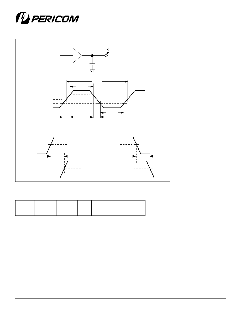
Figure 1. Clock Waveforms
Notes:
1. Maximum rise/fall times are guaranteed at maximum specified load.
2. Minimum rise/fall times are guaranteed at minimum specified load.
3. Rise/fall times are specified with pure capacitive load as shown.
Testing is done with an additional 500
resistor in parallel.
Minimum and Maximum Expected Capacitive Loads
Design Guidelines to Reduce EMI
1. Place series resistors and CI capacitors as close as possible to the respective clock pins. Typical value
for CI is 10pF. Series resistor value can be increased to reduce EMI provided that the rise and fall
time are still within the specified values.
2. Minimize the number of vias of the clock traces.
3. Route clock traces over a continuous ground plane or over a continuous power plane. Avoid routing
clock traces from plane to plane (refer to rule #2).
4. Position clock signals away from signals that go to any cables or any external connectors.
k
c
o
l
C
d
a
o
L
.
n
i
M
d
a
o
L
.
x
a
M
s
ti
n
U
s
e
t
o
N
M
A
R
D
S
5
1
0
2
F
p
n
o
it
a
ci
fi
c
e
p
S
M
M
I
D
M
A
R
D
S