Transistors with built-in Resistor
1
Publication date: December 2003
SJH00010CED
UNR221x Series
(UN221x Series)
Silicon NPN epitaxial planar transistor
For digital circuits
Features
· Costs can be reduced through downsizing of the equipment and
reduction of the number of parts.
· Mini type package allowing easy automatic insertion through tape
packing and magazine packing
Resistance by Part Number
Marking Symbol (R
1
)
(R
2
)
· UNR2210 (UN2210)
8L
47 k
· UNR2211 (UN2211)
8A
10 k
10 k
· UNR2212 (UN2212)
8B
22 k
22 k
· UNR2213 (UN2213)
8C
47 k
47 k
· UNR2214 (UN2214)
8D
10 k
47 k
· UNR2215 (UN2215)
8E
10 k
· UNR2216 (UN2216)
8F
4.7 k
· UNR2217 (UN2217)
8H
22 k
· UNR2218 (UN2218)
8I
0.51 k
5.1 k
· UNR2219 (UN2219)
8K
1 k
10 k
· UNR221D (UN221D)
8M
47 k
10 k
· UNR221E (UN221E)
8N
47 k
22 k
· UNR221F (UN221F)
8O
4.7 k
10 k
· UNR221K (UN221K)
8P
10 k
4.7 k
· UNR221L (UN221L)
8Q
4.7 k
4.7 k
· UNR221M (UN221M)
EL
2.2 k
47 k
· UNR221N (UN221N)
EX
4.7 k
47 k
· UNR221T (UN221T)
EZ
22 k
47 k
· UNR221V (UN221V)
FD
2.2 k
2.2 k
· UNR221Z (UN221Z)
FF
4.7 k
22 k
Absolute Maximum Ratings T
a
= 25°C
B
R
1
R
2
C
E
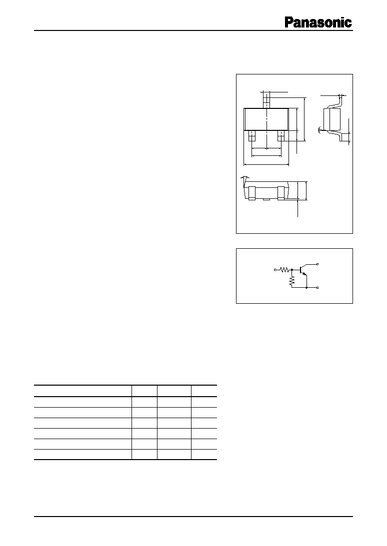
Internal Connection
Unit: mm
1: Base
2: Emitter
3: Collector
EIAJ: SC-59
Mini3-G1 Package
0.40
+0.10
0.05
(0.65)
1.50
+0.25 0.05
2.8
+0.2 0.3
2
1
3
(0.95) (0.95)
1.9
±0.1
2.90
+0.20
0.05
0.16
+0.10
0.06
0.4
±
0.2
5°
10°
0 to 0.1
1.1
+0.2 0.1
1.1
+0.3 0.1
Note) The part numbers in the parenthesis show conventional part number.
Parameter
Symbol
Rating
Unit
Collector-base voltage (Emitter open)
V
CBO
50
V
Collector-emitter voltage (Base open)
V
CEO
50
V
Collector current
I
C
100
mA
Total power dissipation
P
T
200
mW
Junction temperature
T
j
150
°C
Storage temperature
T
stg
-55 to +150
°C

UNR221x Series
2
SJH00010CED
Electrical Characteristics T
a
= 25°C ± 3°C
Parameter
Symbol
Conditions
Min
Typ
Max
Unit
Collector-base voltage (Emitter open)
V
CBO
I
C
= 10 µA, I
E
= 0
50
V
Collector-emitter voltage (Base open)
V
CEO
I
C
= 2 mA, I
B
= 0
50
V
Collector-base cutoff current (Emitter open)
I
CBO
V
CB
= 50 V, I
E
= 0
0.1
µA
Collector-emitter cutoff current (Base open)
I
CEO
V
CE
= 50 V, I
B
= 0
0.5
µA
Emitter-base
UNR2210/2215/2216/2217
I
EBO
V
EB
= -6 V, I
C
= 0
0.01
mA
cutoff current UNR2213
0.1
(Collector open) UNR2212/2214/221D/
0.2
221E/221M/221N/221T
UNR221Z
0.4
UNR2211
0.5
UNR221F/221K
1.0
UNR2219
1.5
UNR2218/221L/221V
2.0
Forward current
UNR221V
h
FE
V
CE
= 10 V, I
C
= 5 mA
6
20
transfer ratio
UNR2218/221K/221L
20
UNR2219/221D/221F
30
UNR2211
35
UNR2212/221E
60
UNR221Z
60
200
UNR2213/2214/221M
80
UNR221N/221T
80
400
UNR2210
*
/2215
*
/2216
*
/2217
*
160
460
Collector-emitter saturation voltage
V
CE(sat)
I
C
= 10 mA, I
B
= 0.3 mA
0.25
V
UNR221V
I
C
= 10 mA, I
B
= 1.5 mA
Output voltage high-level
V
OH
V
CC
= 5 V, V
B
= 0.5 V, R
L
= 1 k
4.9
V
Output voltage low-level
V
OL
V
CC
= 5 V, V
B
= 2.5 V, R
L
= 1 k
0.2
V
UNR2213/221K
V
CC
= 5 V, V
B
= 3.5 V, R
L
= 1 k
UNR221D
V
CC
= 5 V, V
B
= 10 V, R
L
= 1 k
UNR221E
V
CC
= 5 V, V
B
= 6 V, R
L
= 1 k
Transition frequency
f
T
V
CB
= 10 V, I
E
= -2 mA, f = 200 MHz
150
MHz
Input resistance
UNR2218
R
1
-30%
0.51
+30%
k
UNR2219
1.0
UNR221M/211V
2.2
UNR2216/221F/221L/
4.7
221N/221Z
UNR2211/2214/2215/221K
10
UNR2212/2217/221T
22
UNR2210/2213/221D/221E
47
Rank
Q
R
S
No-rank
h
FE
160 to 260
210 to 340
290 to 460
160 to 460
Note) 1. Measuring methods are based on JAPANESE INDUSTRIAL STANDARD JIS C 7030 measuring methods for transistors.
2. *: Rank classification
UNR221x Series
3
SJH00010CED
Electrical Characteristics (continued) T
a
= 25°C ± 3°C
Parameter
Symbol
Conditions
Min
Typ
Max
Unit
Resistance ratio UNR221M
R
1
/R
2
0.047
UNR221N
0.1
UNR2218/2219
0.08
0.10
0.12
UNR221Z
0.21
UNR2214
0.17
0.21
0.25
UNR221T
0.47
UNR221F
0.37
0.47
0.57
UNR221V
1.0
UNR2211/2212/2213/221L
0.8
1.0
1.2
UNR221K
1.70
2.13
2.60
UNR221E
1.70
2.14
2.60
UNR221D
3.7
4.7
5.7
I
C
V
CE
V
CE(sat)
I
C
h
FE
I
C
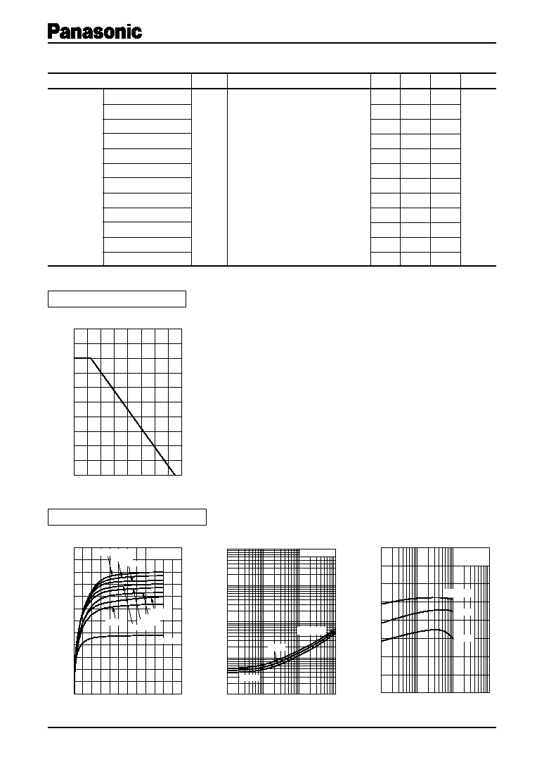
Common characteristics chart
P
T
T
a
Characteristics charts of UNR2210
0
50
100
150
200
250
0
40
80
120
160
Ambient temperature T
a
(
°C)
Total power dissipation P
T
(mW
)
Note) Measuring methods are based on JAPANESE INDUSTRIAL STANDARD JIS C 7030 measuring methods for transistors.
0
12
2
10
4
8
6
0
60
50
40
30
20
10
Collector-emitter voltage V
CE
(V)
Collector current I
C
(mA)
T
a
= 25°C
I
B
= 1.0 mA
0.1 mA
0.3 mA
0.4 mA
0.5 mA
0.6 mA
0.7 mA
0.8 mA
0.9 mA
0.01
0.1
0.1
1
10
100
1
10
100
Collector-emitter saturation voltage V
CE(sat)
(V)
Collector current I
C
(mA)
I
C
/ I
B
= 10
T
a
= 75°C
25
°C
-25°C
0
1
100
200
300
400
10
100
1 000
Forward current transfer ratio h
FE
Collector current I
C
(mA)
V
CE
= 10 V
T
a
= 75°C
25
°C
-25°C
UNR221x Series
4
SJH00010CED
I
C
V
CE
V
CE(sat)
I
C
h
FE
I
C
C
ob
V
CB
I
O
V
IN
V
IN
I
O
C
ob
V
CB
I
O
V
IN
V
IN
I
O
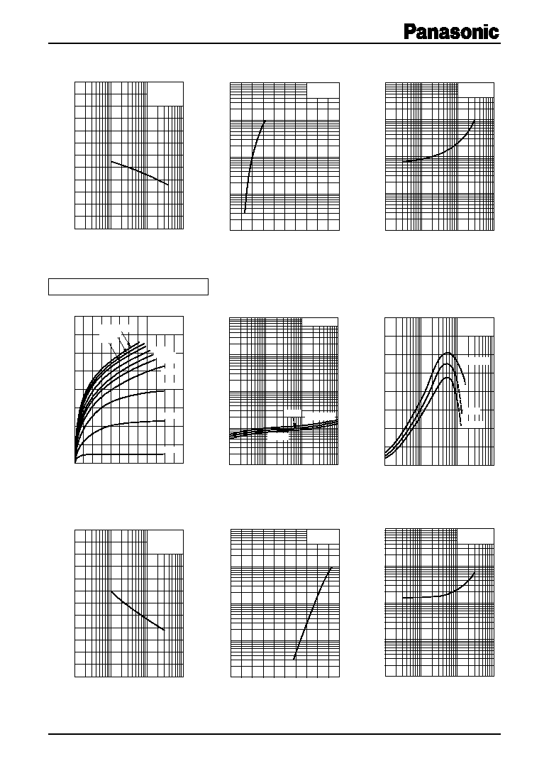
Characteristics charts of UNR2211
0
0.1
6
5
4
3
2
1
1
10
100
Collector output capacitance
(Common base, input open circuited)
C
ob
(pF)
Collector-base voltage V
CB
(V)
f
= 1 MHz
I
E
= 0
T
a
= 25°C
1
0.4
10
10
2
10
3
10
4
1.4
1.2
1.0
0.8
0.6
Output current I
O
(
µ
A)
Input voltage V
IN
(V)
V
O
= 5 V
T
a
= 25°C
0.01
0.1
0.1
1
10
100
1
10
100
Input voltage V
IN
(V)
Output current I
O
(mA)
V
O
= 0.2 V
T
a
= 25°C
0
0
12
2
10
4
8
6
40
120
80
160
Collector-emitter voltage V
CE
(V)
Collector current I
C
(mA)
T
a
= 25°C
I
B
= 1.0 mA
0.1 mA
0.2 mA
0.3 mA
0.4 mA
0.5 mA
0.6 mA
0.7 mA
0.8 mA
0.9 mA
0.01
0.1
0.1
1
10
100
1
10
100
I
C
/ I
B
= 10
T
a
= 75°C
25
°C
-25°C
Collector-emitter saturation voltage V
CE(sat)
(V)
Collector current I
C
(mA)
0
1
100
200
300
400
10
100
1 000
V
CE
= 10 V
T
a
= 75°C
25
°C
-25°C
Forward current transfer ratio h
FE
Collector current I
C
(mA)
0
0.1
6
5
4
3
2
1
1
10
100
f
= 1 MHz
I
E
= 0
T
a
= 25°C
Collector output capacitance
(Common base, input open circuited)
C
ob
(pF)
Collector-base voltage V
CB
(V)
1
0.4
10
10
2
10
3
10
4
1.4
1.2
1.0
0.8
0.6
Output current I
O
(
µ
A)
Input voltage V
IN
(V)
V
O
= 5 V
T
a
= 25°C
0.01
0.1
0.1
1
10
100
1
10
100
Input voltage V
IN
(V)
Output current I
O
(mA)
V
O
= 0.2 V
T
a
= 25°C
UNR221x Series
5
SJH00010CED
I
C
V
CE
V
CE(sat)
I
C
h
FE
I
C
I
C
V
CE
V
CE(sat)
I
C
h
FE
I
C
C
ob
V
CB
I
O
V
IN
V
IN
I
O
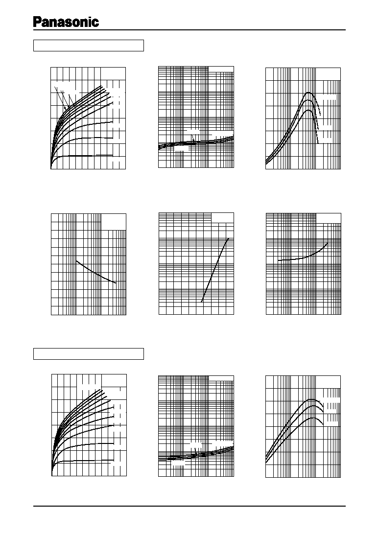
Characteristics charts of UNR2212
Characteristics charts of UNR2213
0
0
12
2
10
4
8
6
40
120
80
160
Collector-emitter voltage V
CE
(V)
Collector current I
C
(mA)
T
a
= 25°C
I
B
= 1.0 mA
0.1 mA
0.2 mA
0.3 mA
0.4 mA
0.5 mA
0.6 mA
0.7 mA
0.9 mA
0.8 mA
0.01
0.1
0.1
1
10
100
1
10
100
Collector-emitter saturation voltage V
CE(sat)
(V)
Collector current I
C
(mA)
I
C
/ I
B
= 10
T
a
= 75°C
25
°C
-25°C
0
1
100
200
300
400
10
100
1 000
Forward current transfer ratio h
FE
Collector current I
C
(mA)
V
CE
= 10 V
T
a
= 75°C
25
°C
-25°C
0
0.1
6
5
4
3
2
1
1
10
100
Collector output capacitance
(Common base, input open circuited)
C
ob
(pF)
Collector-base voltage V
CB
(V)
f
= 1 MHz
I
E
= 0
T
a
= 25°C
1
0.4
10
10
2
10
3
10
4
1.4
1.2
1.0
0.8
0.6
Output current I
O
(
µ
A)
Input voltage V
IN
(V)
V
O
= 5 V
T
a
= 25°C
0.01
0.1
0.1
1
10
100
1
10
100
Input voltage V
IN
(V)
Output current I
O
(mA)
V
O
= 0.2 V
T
a
= 25°C
0
0
12
2
10
4
8
6
40
120
80
160
Collector-emitter voltage V
CE
(V)
Collector current I
C
(mA)
T
a
= 25°C
I
B
= 1.0 mA
0.1 mA
0.2 mA
0.3 mA
0.4 mA
0.5 mA
0.6 mA
0.7 mA
0.8 mA
0.9 mA
0.01
0.1
0.1
1
10
100
1
10
100
Collector-emitter saturation voltage V
CE(sat)
(V)
Collector current I
C
(mA)
I
C
/ I
B
= 10
T
a
= 75°C
25
°C
-25°C
0
1
100
200
300
400
10
100
1 000
Forward current transfer ratio h
FE
Collector current I
C
(mA)
V
CE
= 10 V
T
a
= 75°C
25
°C
-25°C