1
A/D, D/C Converters for Image Signal Processing
MN6570F, MN6570TF, and MN6570EF
Low Power 8-Bit, 3-Channel CMOS D/A Converters for Image Processing
Overview
The MN6570F, MN6570TF, and MN6570EF are high-
speed 8-bit, 3-channel CMOS digital-to-analog convert-
ers with maximum conversion rates of 35 MSPS, 40
MSPS, and 40 MSPS, respectively.
They use both a matrix cell and weighted current tech-
nology.
The three channels use separate clock signals, so they
may be used as totally independent D/A converters.
Features
Maximum conversion rate:
MN6570F: 35MSPS (min.)
MN6570TF and MN6570EF: 40 MSPS (min.)
Linearity error:
±
0.2 LSB (typ.)
Differential linearity error:
±
0.2 LSB (typ.)
Power supply voltage: V
CC
= 5.0
±
0.5 V
Power consumption:
MN6570F: 340 mW (typ.)
MN6570TF and MN6570EF: 190 mW (typ.)
Full scale current:
MN6570F: 13 mA (typ.)
MN6570TF and MN6570EF: 5 mA (typ.)
Applications
Digital television
Digital video equipment
Digital image processing equipment
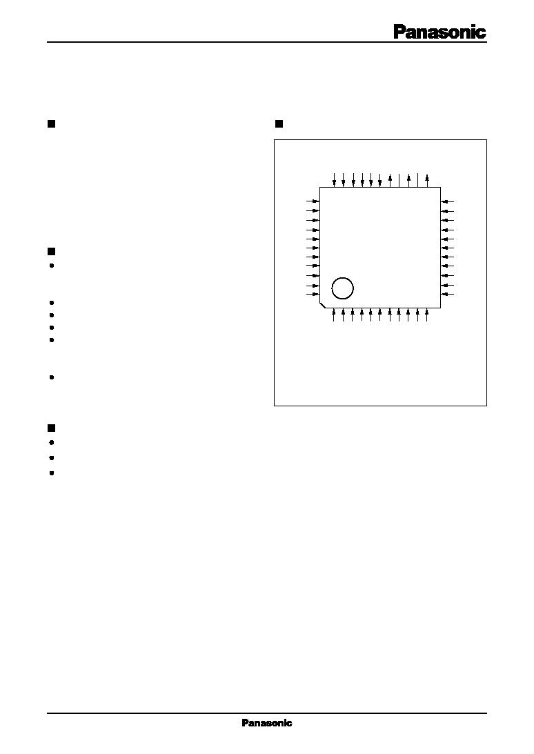
Pin Assignment
QFP044-P-1010
(TOP VIEW)
DG4
DG3
DG2
DG1
CLKG
DV
SS
DV
DD
DR8
DR7
DR6
DR5
DB5
DB6
DB7
DB8
AV
SS
AV
SS
I
OB
N.C.
I
OG
N.C.
I
OR
VIB
COMP
V
REF
I
REF
AV
DD
AV
DD
CLKR
DR1
DR2
DR3
DR4
DB4
DB3
DB2
DB1
CLKB
DV
SS
DV
DD
DG8
DG7
DG6
DG5
1
2
3
4
5
6
7
8
9
10
11
22
21
20
19
18
17
16
15
14
13
12
34
35
36
37
38
39
40
41
42
43
44
33
32
31
30
29
28
27
26
25
24
23
2
MN6570F, MN6570TF, MN6570EF
A/D, D/C Converters for Image Signal Processing
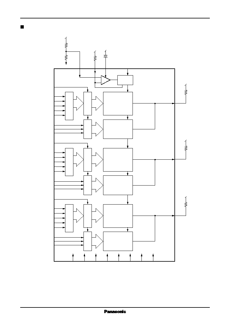
Block Diagram
16
15
14
13
12
11
10
9
8
5
4
3
2
1
44
43
42
41
38
37
36
35
34
33
32
DB6
DB2
DG7
DG6
DG5
DG4
DG3
DG2
DR7
DR6
DR5
DR4
DR3
DR2
CLKG
DB3
DB4
DB5
DB7
(LSB)DB8
(MSB)DB1
(LSB)DG8
(MSB)DG1
(LSB)DR8
(MSB)DR1
31
30
23
25
27
17
18
28
29
7
40
6
39
20
19
21
22
24
26
V
REF
I
REF
R
REF
COMP
I
OR
I
OG
I
OB
R
OUT
R
OUT
R
OUT
AV
DD
AV
DD
DV
DD
DV
DD
DV
SS
DV
SS
AV
SS
AV
SS
VIB
N.C.
N.C.
C
COMP
+
CLKB
CLKR
+
Current
Source
Weighted
Current Cell
Weighted
Current Cell
Weighted
Current Cell
Matrix
Cell
Matrix
Cell
Matrix
Cell
Latch
Latch
Latch
Latch
Latch
Latch
Decoder
Decoder
Decoder

3
A/D, D/C Converters for Image Signal Processing
MN6570F, MN6570TF, MN6570EF
Pin Descriptions
Pin No.
Symbol
Function Description
1
DG4
G signal digital input
2
DG3
G signal digital input
3
DG2
G signal digital input
4
DG1
G signal digital input (MSB)
5
CLKG
G signal sampling clock
6
DV
SS
Ground for digital circuits
7
DV
DD
Power supply for digital circuits
8
DR8
R signal digital input (LSB)
9
DR7
R signal digital input
10
DR6
R signal digital input
11
DR5
R signal digital input
12
DR4
R signal digital input
13
DR3
R signal digital input
14
DR2
R signal digital input
15
DR1
R signal digital input (MSB)
16
CLKR
R signal sampling clock
17
AV
DD
Power supply for analog circuits
18
AV
DD
Power supply for analog circuits
19
I
REF
Full scale adjustment resistor
20
V
REF
Reference voltage input
21
COMP
Phase compensation
22
VIB
Capacitor connection
23
I
OR
R signal analog current output
24
N.C.
No connection
25
I
OG
G signal analog current output
26
N.C.
No connection
27
I
OB
B signal analog current output
28
AV
SS
Ground for analog circuits
29
AV
SS
Ground for analog circuits
30
DB8
B signal digital input (LSB)
31
DB7
B signal digital input
32
DB6
B signal digital input
33
DB5
B signal digital input
34
DB4
B signal digital input
35
DB3
B signal digital input
36
DB2
B signal digital input
37
DB1
B signal digital input (MSB)
38
CLKB
B signal sampling clock
39
DV
SS
Ground for digital circuits
40
DV
DD
Power supply for digital circuits

4
MN6570F, MN6570TF, MN6570EF
A/D, D/C Converters for Image Signal Processing
Pin Descriptions (continued)
Pin No.
Symbol
Function Description
41
DG8
G signal digital input (LSB)
42
DG7
G signal digital input
43
DG6
G signal digital input
44
DG5
G signal digital input
Recommended Operating Conditions
V
DD
=AV
DD
=DV
DD
=5.0V, V
SS
=AV
SS
=DV
SS
=0V, Ta=25°C
Parameter
Symbol
min
typ
max
Unit
Power supply voltage
V
DD
4.5
5.0
5.5
V
Reference
MN6570F
V
REF
2.0
2.3
3.5
V
voltage
MN6570TF/EF
2.0
2.42
3.7
Reference
MN6570F
R
REF
390
430
1500
resistance
MN6570TF/EF
820
1100
1400
External compensation capacitor
C
COMP
0.33
1.0
3.3
µ
F
Output load
MN6570F
R
OUT
50
75
330
resistance
MN6570TF/EF
300
400
500
Digital input
"H" level
V
IH
2.4
--
V
DD
V
voltage
"L" level
V
IL
V
SS
--
0.8
V
Clock
"H" level pulse width
t
WH
10
--
--
ns
"L" level pulse width
t
WL
10
--
--
ns
Absolute Maximum Ratings
Ta=25°C
Parameter
Symbol
Rating
Unit
Power supply voltage for digital circuits
DV
DD
0.3 to +7.0
V
Power supply voltage for analog circuits
AV
DD
0.3 to +7.0
V
Input voltage
V
I
DV
SS
0.3 to DV
DD
+0.3
V
Output voltage
V
O
AV
SS
0.3 to AV
DD
+0.3
V
Operating ambient temperature
T
opr
20 to +70
*1
/20 to +75
*2
/30 to 85
*3
°C
Storage temperature
T
stg
55 to +125
°C
*1 MN6570F
*2 MN6570TF
*3 MN6570EF

5
A/D, D/C Converters for Image Signal Processing
MN6570F, MN6570TF, MN6570EF
Electrical Characteristics
DV
DD
=AV
DD
=5.0V, DV
SS
=AV
SS
=0V, Ta=25°C
·
MN6570F
Parameter
Symbol Conditions
min
typ
max
Unit
Power supply current
I
DD
V
DD
=5.0V, t
CLK
=35MHz,
R
OUT
=75
, Output amplitude =1 V,
68
85
mA
T=25°C
Resolution
RES
8
bit
Linearity error
E
L
V
DD
=5.0V, R
OUT
=75
±
0.2
±
0.5
LSB
Differential linearity error
E
D
R
REF
=430
±
0.2
±
0.5
LSB
Full scale current
I
FS
V
REF
=2.3V
13
mA
Setup time
t
S
8
ns
Hold time
t
H
8
ns
Settling time
t
ST
V
DD
=5.0V, R
OUT
=75
20
28
ns
Maximum conversion speed
F
C(max.)
R
REF
=430
V
REF
=2.3V
35
50
MSPS
Analog output delay
t
d
5
ns
·
MN6570TF, MN6570EF
Parameter
Symbol Conditions
min
typ
max
Unit
Power supply current
I
DD
V
DD
=5.0V, t
CLK
=40MHz,
R
OUT
=400
, Output amplitude =2V,
38
55
mA
T=25°C
Resolution
RES
8
bit
Linearity error
E
L
V
DD
=5.0V, R
OUT
=400
±
0.2
±
0.5
LSB
Differential linearity error
E
D
R
REF
=1100
±
0.2
±
0.5
LSB
Full scale current
I
FS
V
REF
=2.42V
5
mA
Setup time
t
S
8
ns
Hold time
t
H
8
ns
Settling time
t
ST
V
DD
=5.0V, R
OUT
=400
20
25
ns
Maximum conversion speed
F
C(max.)
R
REF
=1100
V
REF
=2.42V
40
50
MSPS
Analog output delay time
t
d
5
ns