1
A/D, D/C Converters for Image Signal Processing
MN65702H
Low Power 8-Bit, 3-Channel CMOS D/A Converter for Image Processing
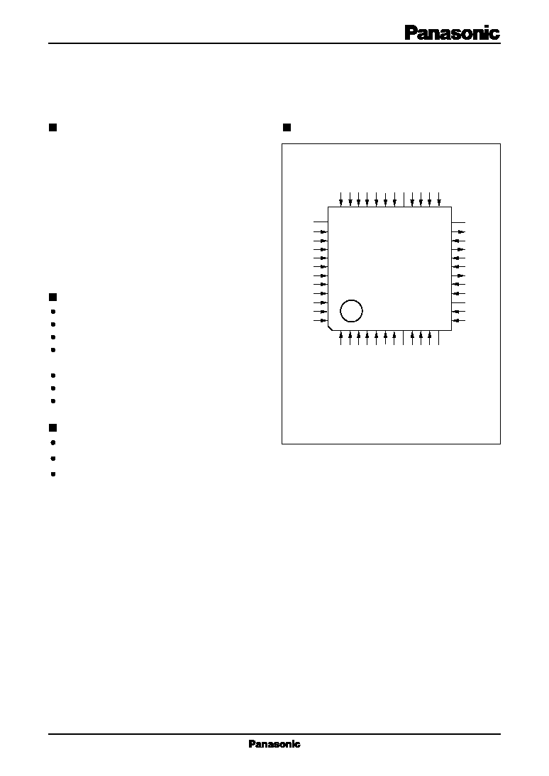
Pin Assignment
Overview
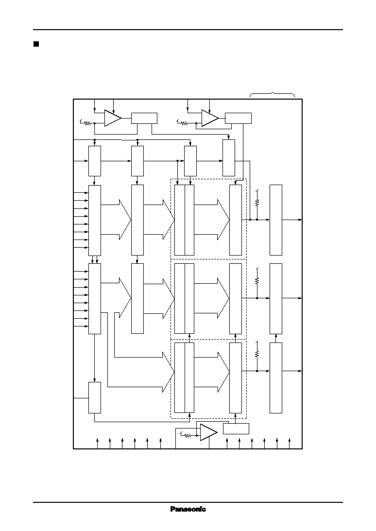
The MN65702H is a high-speed 8-bit, 3-channel CMOS
digital-to-analog converter. (Two channels use serial in-
put.)
It uses both a matrix cell and weighted current technol-
ogy to achieve both low power consumption and high
speed.
It features built-in output resistor, reference resistor, and
low pass filter, and provides independent output ampli-
tude adjustment for the Y (luminance) and C (chroma)
synchronization signals. The Y (luminance signal) can
be superimposed with an external SYNC signal.
Features
Maximum conversion rate: 20 MSPS (min.)
Linearity error:
±
0.2 LSB (typ.)
Differential linearity error:
±
0.2 LSB (typ.)
Power supply voltage: V
DD
= 3.3
±
0.3 V, V
CC
= 4.8
±
0.3 V
Full scale current: 2.33 mA (typ.)
Power consumption: 100 mW (typ.) (f
CLK
=15 MHz)
Built-in LPF and synchronization function.
Applications
Digital television
Digital video equipment
Digital image processing equipment
QFH048-P-0707
(TOP VIEW)
DY4
DY3
DY2
DY1
SYNC
V
CC
DV
SS
N.C.
N.C.
AV
DD
COMPS
N.C.
DC4
DC5
DC6
DC7
DC8
DV
SS
DV
DD
N.C.
AV
SS
V
REFC
N.C.
COMPC
N.C.
V
OUT
V
CC
U
OUT
AV
SS
V
CC
Y
OUT
AV
SS
V
REFY
N.C.
COMPY
V
REFS
N.C.
DC3
DC2
DC1
UV
SEL
DV
DD
DV
SS
CLK
DY8
DY7
DY6
DY5
1
2
3
4
5
6
7
8
9
10
11
12
24
23
22
21
20
19
18
17
16
15
14
13
37
38
39
40
41
42
43
44
45
46
47
48
36
35
34
33
32
31
30
29
28
27
26
25
2
MN65702H
A/D, D/C Converters for Image Signal Processing
Block Diagram
44
V
REFS
V
REFY
COMPS
COMPY
13
11
16
14
5
4
3
2
1
48
47
46
45
40
39
38
36
35
34
33
32
41
6
7
31
43
27
25
10
19
22
17
20
28
30
42
18
21
23
Y
OUT
U
OUT
V
OUT
CLK
SYNC
DY1
DY2
DY3
DY4
DY5
DY6
DY7
DY8
DC1
DC2
DC3
DC4
DC5
DC6
DC7
DC8
UVSEL
COMPC
V
CC
DV
DD
DV
DD
DV
SS
DV
SS
DV
SS
V
REFC
AV
CC
V
CC
V
CC
AV
SS
AV
SS
AV
SS
N.C.
+
+
Current
Source
Current
Source
Current
Source
Latch
Latch
Latch
Latch
Latch
Latch
Latch
Latch
Latch
Latch
Latch
Current cell
Current cell
Current cell
Current cell
Decoder
Decoder
Decoder
+
Low pass filter
Low pass filter
Low pass filter
12
37
29
26
24
15
9
8
3
A/D, D/C Converters for Image Signal Processing
MN65702H
Pin Descriptions
Pin No.
Symbol
Function Description
1
DY4
Y (luminance) digital input
2
DY3
Y (luminance) digital input
3
DY2
Y (luminance) digital input
4
DY1
Y (luminance) digital input (MSB)
5
SYNC
SYNC signal judgment signal
6
V
CC
Filter power supply for analog circuits
7
DV
SS
Ground for digital circuits
8
N.C.
No connection
9
N.C.
No connection
10
AV
DD
Power supply for analog circuits
11
COMPS
Phase compensation
12
N.C.
No connection
13
V
REFS
SYNC reference voltage input
14
COMPY
Phase compensation
15
N.C.
No connection
16
V
REFY
Luminance reference voltage input
17
AV
SS
Ground for analog circuits
18
Y
OUT
Y signal analog current output
19
V
CC
Filter power supply for analog circuits
20
AV
SS
Ground for analog circuits
21
U
OUT
U signal analog current output
22
V
CC
Filter power supply for analog circuits
23
V
OUT
V signal analog current output
24
N.C.
No connection
25
COMPC
Phase compensation
26
N.C.
No connection
27
V
REFC
Chroma reference voltage input
28
AV
SS
Ground for analog circuits
29
N.C.
No connection
30
DV
DD
Power supply voltage for digital circuits
31
DV
SS
Ground for digital circuits
32
DC8
C (chroma) digital input (LSB)
33
DC7
C (chroma) digital input
34
DC6
C (chroma) digital input
35
DC5
C (chroma) digital input
36
DC4
C (chroma) digital input
37
N.C.
No connection
38
DC3
C (chroma) digital input
39
DC2
C (chroma) digital input
40
DC1
C (chroma) digital input (MSB)
41
UVSEL
U/V signal discrimination for C (chroma) signal
42
DV
DD
Power supply voltage for digital circuits

4
MN65702H
A/D, D/C Converters for Image Signal Processing
Absolute Maximum Ratings
Ta=25°C
Parameter
Symbol
Rating
Unit
Power supply voltage
DV
DD
/AV
DD
0.3 to +7.0
V
Power supply voltage for analog circuits
V
CC
0.3 to +7.0
V
Input voltage
V
I
0.3 to DV
DD
+0.3
V
Output voltage
V
O
0.3 to AV
DD
+0.3
V
Operating ambient temperature
T
opr
20 to +70
°C
Storage temperature
T
stg
55 to +125
°C
Pin Descriptions (continued)
Pin No.
Symbol
Function Description
43
DV
SS
Power supply for digital circuits
44
CLK
Sampling clock
45
DY8
Y (luminance) digital input (LSB)
46
DY7
Y (luminance) digital input
47
DY6
Y (luminance) digital input
48
DY5
Y (luminance) digital input
Recommended Operating Conditions
V
DD
=AV
DD
=DV
DD
=3.3V, V
CC
=4.8V, V
SS
=AV
SS
=DV
SS
=0V, Ta=25°C
Parameter
Symbol
min
typ
max
Unit
Power supply voltage
V
CC
4.5
4.8
5.1
V
V
DD
3.0
3.3
3.6
V
Reference voltage
V
REFS/Y/C
--
2.15/1.96/1.93
--
V
External compensation capacitor
C
COMPS, Y, C
0.33
1.0
3.3
µ
F
Digital input
"H" level
V
IH
2.4
--
V
DD
V
voltage
"L" level
V
IL
V
SS
--
0.8
V
Clock
"H" level pulse width
t
WH
20
--
--
ns
"L" level pulse width
t
WL
20
--
--
ns
Electrical Characteristics
DV
DD
=AV
DD
=3.0V, V
CC
=4.8V, DV
SS
=AV
SS
=0V, Ta=25°C
Parameter
Symbol Conditions
min
typ
max
Unit
Power supply voltage
I
DD
/I
CC
f
CLK
=15MHz,
--
12/12
21/21
mA
Output amplitude = 0.7 V,
Resolution
RES
--
8
--
bit
Linearity error
E
L
V
DD
=3.3V, V
CC
=4.8V
--
±
0.2
±
0.5
LSB
Differential linearity error
E
D
Y (luminance) output amplitude =0.7V
p-p
--
±
0.2
±
0.5
LSB
Full scale current
I
FS
C (chroma) output amplitude =0.7V
p-p
--
2.33
--
mA
Setup time
t
S
15
--
--
ns
Hold time
t
H
5
--
--
ns
Settling time
t
ST
V
DD
=3.3V, V
CC
=4.8V
--
30
50
ns
Maximum conversion speed
F
C(max.)
Y·C output amplitude =0.7V
PP
20
--
--
MSPS
Analog output delay time
t
dY
/t
dc
f=100kHz
--
90/140
--
ns

5
A/D, D/C Converters for Image Signal Processing
MN65702H
Timing Chart
Filter Characteristics
DV
DD
=AV
DD
=3.0V, V
CC
=4.8V, DV
SS
=AV
SS
=0V, Ta=25°C
Parameter
Symbol
Conditions
min
typ
max
Unit
Y filter I/O gain
GYF
f=100kHz
1.2
0.2
0.8
dB
Y filter f characteristic (fck/2)
FYFCK
f=100kHz
6.35MHz
10
7
4
dB
Y filter f characteristic (3MHz)
FYFCL
f=100kHz
3.0MHz
3
1
1.0
dB
Y filter group delay
DYF
f=100kHz
60
80
100
dB
UV filter I/O gain
GCF
f=100kHz
1.2
0.2
0.8
dB
UV filter f characteristic (fck/4)
FCFCK
f=100kHz
3.18MHz
15
10
6
dB
UV filter f characteristic (1MHz)
FCFCL
f=100kHz
1.0MHz
3
1
1.0
dB
UV filter group delay
DCF
f=100kHz
100
130
160
ns
M SELECT = "H," Y and U(C), 3-channel output
SYNC
CLK
DY1 to DY8
DC1 to DC8
UVSEL
Y
OUT
U
OUT
V
OUT
Two clock cycles
Two clock cycles
Y-1
Y-2
Y-2
U-4
V-4
V-2
V0
V2
U-2
U0
U2
Y-1
U0
U2
U4
V0
Y0
Y1
Y3
V2
V4
Y0
Y1
Y2
Y3
Y4
Y5
t
ds
t
d
t
ds
: SYNC delay time
t
d
: Analog output delay time
t
st
: Settling time
t
st
t
ds