Under
Development
MIP2C2 High-Performance IPD for Battery Chargers
I Overview
MIP2C2 is a high-performance IPD designed for 7W battery chargers. It
features built-in protection circuits necessary for compact power source charger
circuitry. This allows a significant reduction in externally connected parts.
MIP2C2 provides PWM control when a normal load is applied and intermittent
control with low load. This results in greater efficiency for very low to maximum
loads, while also conserving power during standby.
I Features
G Built-in charge protection circuit
Built-in overcurrent, overheating, load shorting and overvoltage protection circuits
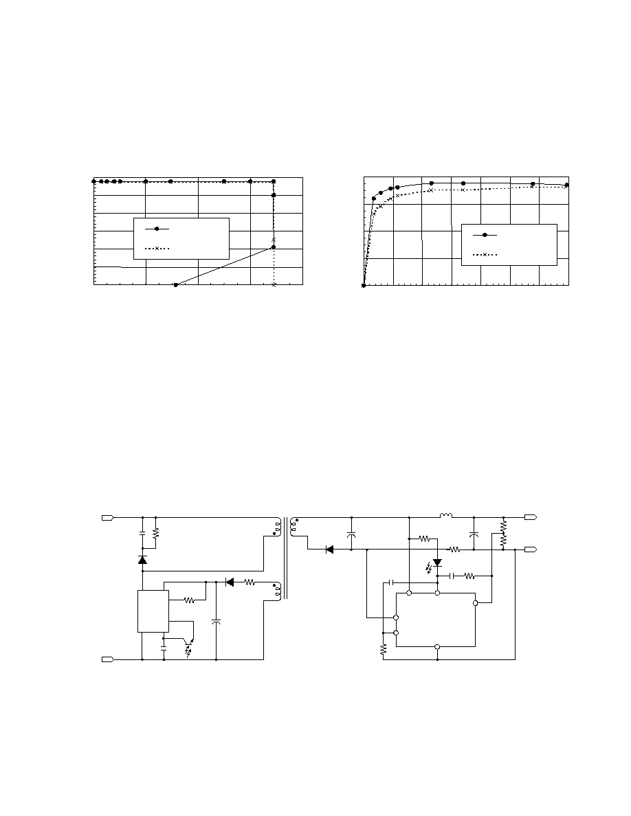
G Significantly reduced power consumption with no load*
20mW at 100VAC, 25mW at 240VAC
G High efficiency with rated load*
75% at 100VAC,72% at 240VAC
G Reduced number of parts (12 less than conventional Panasonic models)
* With worldwide input and 5.8V/0.7A output
I Applications
G Chargers (for cellular phones, etc. )
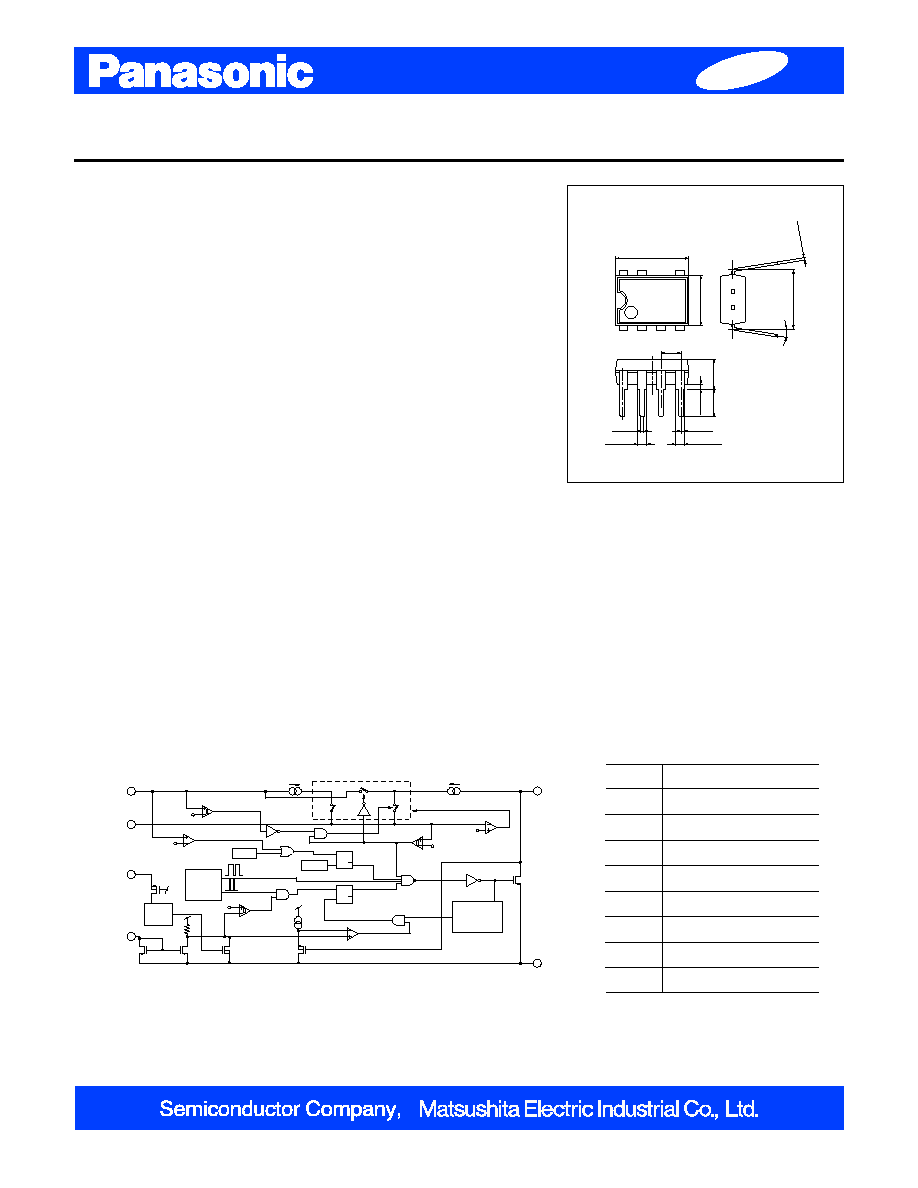
I Block Diagram
I Pin Descriptions
1 Kotari-yakemachi, Nagaokakyo, Kyoto 617-8520, Japan
Tel. (075) 951-8151
http://www.panasonic.co.jp/semicon/
New publication, effective from Jan. 25. 2002.
E00107AE
� The products and specifications are subject to change without any notice. Please ask for the latest product standards to guarantee the satisfaction of your product requirements.
Saves power during standby, enhances efficiency
3
�
to 15
�
6.3
�
0.2
3.8
�
0.25
3.4
�
0.3
7.62
�
0.25
9.4
�0.3
2.54
�0.25
0.6
+0.25 -
0.01
0.25
+0.10
-
0.05
1.2
�0.25
(2,3,7PIN)
0.5
�0.1
0.6
�0.1
(1,4,5,8PIN)
0.4
�0.1
1
2
3
4
8
7
5
Unit : mm
DIP8-A1(CF)
Pin No.
Function
1
V
DD
2
FB
3
CL
4
V
CC
5
Drain
6
7
Source
8
Source
VCC
5.7V
5.7V
4.7V
Gate driver
Power
MOSFET
VDD
CL
FB
SOURCE
DRAIN
S
R
Q
Q
S
R
Q
Q
Reg.
Restart trigger
Overheat
protection
12V
10V
VCC UV
22V
VCC OVP
Oscillator
Max Duty
Clock
(10 to100%)
15%
20%
Drain current detection
Blanking pulse
circuit
VDD UV
Clamp voltage
variable circuit
Low load detection
Intermittent control

I Absolute Maximum Ratings
Parameters
Symbol
Rating
Unit
Drain voltage
V
D
700
V
Supply voltage
V
CC
30
V
Feedback voltage
V
FB
7
V
CL terminal voltage
V
CL
7
V
Drain current
I
D
500
V
Operating Junction Temperature
T
ch
150
�C
Storage temperature
T
stg
-55 to +150
�C
I Electrical Characteristics (Ta = 25�C � 3�C)
Parameters
Symbol
Conditions
min
typ
max
Unit
( Control Function )
Oscillator output frequency
f
OSC
FB:Open
90
100
110
kHz
Max. Duty cycle
MAXDC
FB:Open
-
50
-
%
VDD reference voltage
V
DD
-
5.7
-
V
VDD stop voltage
V
UV
-
5.1
-
V
Circuit current
I
CC
-
0.5
-
mA
VCC charge start voltage
V
CC(ON)
-
12
-
V
VCC charge stop voltage
V
CC(OFF)
-
10
-
V
VCC charge voltage hysteresis
V
CC
-
2
-
V
VDD charge current
I
ch1
V
DD
= 0V
-
3.0
-
mA
I
ch2
V
DD
= 4V
-
1.5
-
mA
Feedback current
I
FB
-
120
-
�A
Feedback current hystereses
I
FBHYS
-
3
-
�A
LC terminal current
I
CLMAX
20
-
-
�A
LC terminal current
I
CLMIN
-
-
5
�A
(Protection Function)
Overcurrent detection
I
LIMITMIN
I
CL
< I
CLMIN
-
0.05
-
A
I
LIMITMAX
I
CL
> I
CLMAX
-
0.35
-
Overvoltage detection
V
CC(0V)
-
20
-
V
Overheating detection
T
OTP
130
140
150
�C
Latch reset voltage
V
creset
-
3
-
V
(Output Function)
ON resistance
R
DS(ON)
I
D
= 0.1 A
-
22
27
Drain leak current
I
DSS
V
DS
= 630 V
-
-
250
�A
Drain breakdown voltage
V
DSS
I
D
= 0.25 mA
700
-
-
V
Rise time
t
r
-
100
-
ns
Fall time
t
f
-
50
-
ns
(Supply Voltage)
Minimum drain voltage
V
D(MIN)
50
-
-
V