1
ICs for TV
Publication date: November 2001
SDB00080AEB
AN2526NFH
Automotive LCD TV signal processor IC
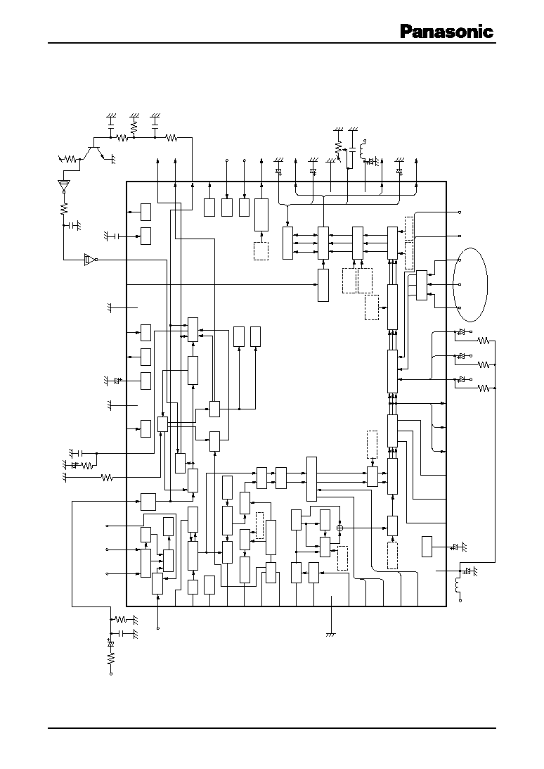
I Overview
The AN2526NFH is a video signal processing IC with
an LCD's 5 V-source driving power supply for TFT color
LCD (normally white type), and it supports NTSC and
PAL systems. The main circuitry of this IC includes video-
signal processing circuit, color signal processing circuit,
interface circuit, synchronizing circuit and many color
quality adjusting circuits. This IC converts the composite
video signal or separated Y/C signal or RGB signals into
RGB signals available for TFT color LCD.
I Features
· Supply voltage: 5 V/7.5 V
· Built-in LCD's 5 V-source driving power supply
· Low consumption power (typ. 260 mW)
· Supporting NTSC and PAL
· Supporting composite, component and color differen-
tial signal input
· Video signalanalog RGB (2 systems)
One is for OSD (analog/digital).
· Each mode setting is possible with 3-wire or I
2
C Bus
control.
· Electronic volume (D/A converter) built in
· Contrast/Brightness/ correction circuit built in
· Horizontal and vertical display position adjustment are
possible by serial control.
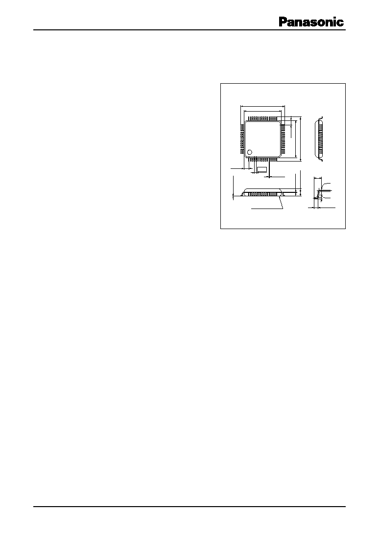
· Package: QFP-64HP10L (10 × 10 × 1.95 mm)
· Difference from the AN2526FH
Compared to the AN2526FH, the sync. system gain is
increased in no signal input. This may cause the picture
on the screen to be swaying horizontally. So we cannot
recommend this IC to be used in the set with no-signal
input mode.
I Applications
· 4 inches to 7 inches middle size TFT LCD equipment
of normally white, of such as in-car TV, an LCD monitor
for car navigation system.
QFP064-P-1010
Unit: mm
10.00
±0.20
48
33
32
17
16
1
64
49
12.00
±0.20
10.00
±
0.20
0.10
±
0.10
12.00
±
0.20
1.95
±
0.20
(1.25)
(1.25)
0.50
0.18
+0.10
-0.05
0.15
+
0.10
-
0.05
Seating plane
(1.00)
0.50
±0.20
0
° to 10°
Note) The package of this product will be changed
to lead-free type (QFP064-P-1010A). See the
new package dimensions section later of this
datasheet.
AN2526NFH
5
SDB00080AEB
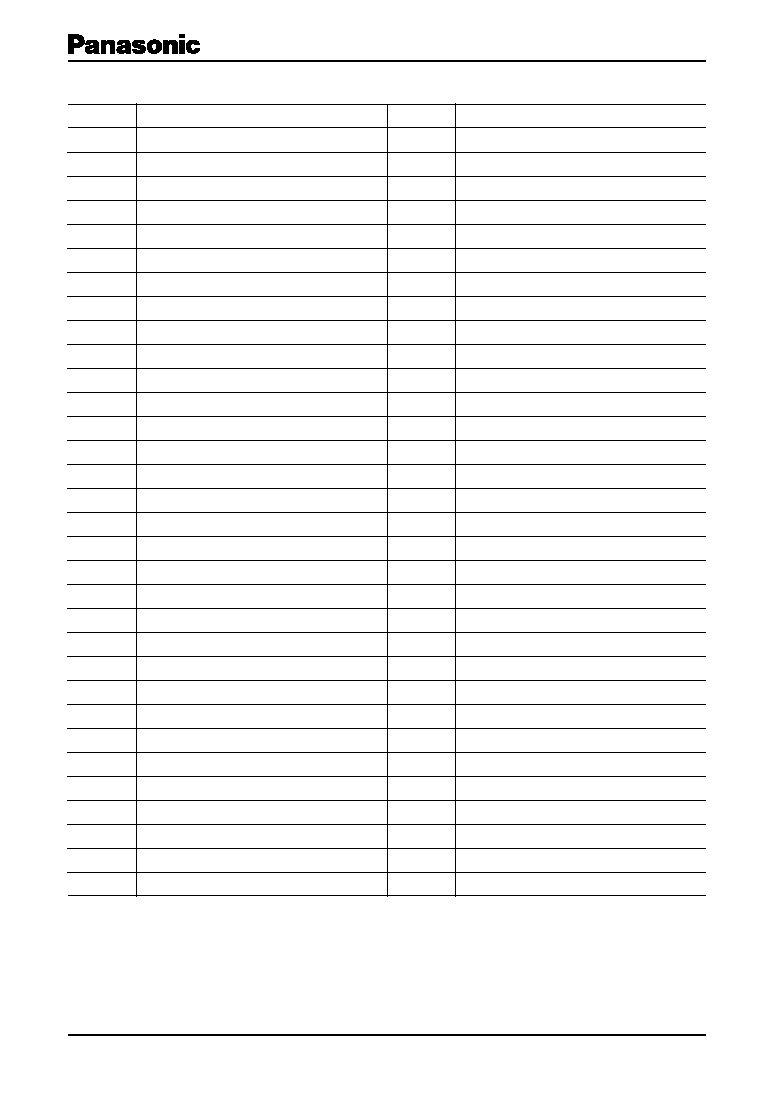
I Pin Descriptions
Pin No.
Description
1
V
CC1
(5.0 V)
2
Reference voltage pin
3
R-ch. clamp detection pin
4
G-ch. clamp detection pin
5
B-ch. clamp detection pin
6
R-ch. decoder output pin
7
G-ch. decoder output pin
8
B-ch. decoder output pin
9
R-ch. analog signal input pin
10
G-ch. analog signal input pin
11
B-ch. analog signal input pin
12
R-ch. analog/character signal input pin
13
G-ch. analog/character signal input pin
14
B-ch. analog/character signal input pin
15
Black level indication control signal input pin
16
Character picking up pulse input pin
17
B-ch. output pin
18
B-ch. output DC feedback detection pin
19
G-ch. output pin
20
V
CC2
(7.5 V)
21
Drive output reference potential input pin
22
GND 1
23
G-ch. output DC feedback detection pin
24
R-ch. output pin
25
R-ch. output DC feedback detection pin
26
Common reverse signal output pin
27
Testing pulse input pin
28
Testing clock input pin
29
Field identification signal output pin
30
Composite synchronous signal output pin
31
Vertical synchronous signal output pin
32
Horizontal synchronous signal output pin
Pin No.
Description
33
PWM output pin
34
Power-on reset detection pin
35
Vertical synchronous signal input pin
36
1H reverse signal input pin
37
Clock-system GND (V
SS
)
38
Clamp pulse input pin
39
DAC monitor pin
40
Clock-system power supply (3.0 V)
41
GND 2
42
Analog imposing control signal input pin
43
AFC loop filter connecting pin
44
VCO frequency adjustment pin
45
Synchronous signal input pin
46
Serial/I
2
C Bus switching pin
47
Serial data shift clock input pin
48
Serial data input pin
49
Serial data write pulse input pin
50
ACC detection pin
51
ACC input pin
52
Horizontal clock detection pin
53
Chroma killer detection pin
54
APC detection pin
55
VXO input pin
56
VXO output pin
57
Y-system clamp detection pin
58
Chroma trap filter connection pin
59
GND 3
60
Luminance signal input pin
61
R-Y output pin
62
B-Y output pin
63
R-Y input pin
64
B-Y input pin