
1
Transistor
2SC3931
Silicon NPN epitaxial planer type
For high-frequency amplification
s
Features
q
Optimum for RF amplification of FM/AM radios.
q
High transition frequency f
T
.
q
S-Mini type package, allowing downsizing of the equipment and
automatic insertion through the tape packing and the magazine
packing.
s
Absolute Maximum Ratings
(Ta=25°C)
Unit: mm
Parameter
Collector to base voltage
Collector to emitter voltage
Emitter to base voltage
Collector current
Collector power dissipation
Junction temperature
Storage temperature
1:Base
2:Emitter
EIAJ:SC70
3:Collector
SMini Type Package
2.1
±
0.1
1.3
±
0.1
0.9
±
0.1
0.7
±
0.1
0.3
+0.1
0
0.15
+0.1
0.05
2.0
±
0.2
1.25
±
0.1
0.425
0.425
1
3
2
0.65
0.2
0.65
0 to 0.1
0.2
±
0.1
Symbol
V
CBO
V
CEO
V
EBO
I
C
P
C
T
j
T
stg
Ratings
30
20
3
15
150
150
55 ~ +150
Unit
V
V
V
mA
mW
°C
°C
s
Electrical Characteristics
(Ta=25°C)
Parameter
Collector to base voltage
Emitter to base voltage
Forward current transfer ratio
Base to emitter voltage
Transition frequency
Common emitter reverse transfer capacitance
Power gain
Noise figure
Symbol
V
CBO
V
EBO
h
FE
*
V
BE
f
T
C
re
PG
NF
Conditions
I
C
= 10
µ
A, I
E
= 0
I
E
= 10
µ
A, I
C
= 0
V
CB
= 6V, I
E
= 1mA
V
CB
= 6V, I
E
= 1mA
V
CB
= 6V, I
E
= 1mA, f = 200MHz
V
CE
= 6V, I
C
= 1mA, f = 10.7MHz
V
CB
= 6V, I
E
= 1mA, f = 100MHz
V
CB
= 6V, I
E
= 1mA, f = 100MHz
min
30
3
65
450
typ
0.72
650
0.8
24
3.3
max
260
1
Unit
V
V
V
MHz
pF
dB
dB
Marking symbol :
U
*
h
FE
Rank classification
Rank
C
D
h
FE
65 ~ 160
100 ~ 260
Marking Symbol
UC
UD

2
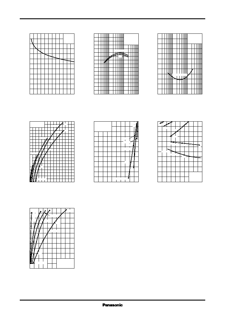
Transistor
2SC3931
P
C
-- Ta
I
C
-- V
CE
I
C
-- I
B
I
C
-- V
BE
V
CE(sat)
-- I
C
h
FE
-- I
C
f
T
-- I
E
Z
rb
-- I
E
C
re
-- V
CE
0
160
40
120
80
140
20
100
60
0
240
200
160
120
80
40
Ambient temperature Ta (°C)
Collector power dissipation P
C
(mW
)
0
18
6
12
0
12
10
8
6
4
2
Ta=25°C
I
B
=100
µ
A
80
µ
A
60
µ
A
40
µ
A
20
µ
A
Collector to emitter voltage V
CE
(V)
Collector current I
C
(mA
)
0
180
60
120
0
12
10
8
6
4
2
V
CE
=6V
Ta=25°C
Base current I
B
(
µ
A)
Collector current I
C
(mA
)
0
2.0
1.6
0.4
1.2
0.8
0
30
25
20
15
10
5
V
CE
=6V
Ta=75°C
25°C
25°C
Base to emitter voltage V
BE
(V)
Collector current I
C
(mA
)
0.1
1
10
100
0.3
3
30
0.01
0.03
0.1
0.3
1
3
10
30
100
I
C
/I
B
=10
Ta=75°C
25°C
25°C
Collector current I
C
(mA)
Collector to emitter saturation voltage V
CE(sat)
(V
)
0.1
1
10
100
0.3
3
30
0
360
300
240
180
120
60
V
CE
=6V
Ta=75°C
25°C
25°C
Collector current I
C
(mA)
Forward current transfer ratio h
FE
0.1
1
10
100
0.3
3
30
0
1200
1000
800
600
400
200
V
CB
=6V
Ta=25°C
Emitter current I
E
(mA)
Transition frequency f
T
(MHz
)
0.1
0.3
1
3
10
0
120
100
80
60
40
20
V
CB
=6V
f=2MHz
Ta=25°C
Emitter current I
E
(mA)
Reverse transfer impedance Z
rb
(
)
0.1
1
10
100
0.3
3
30
0
2.4
2.0
1.6
1.2
0.8
0.4
I
C
=1mA
f=10.7MHz
Ta=25°C
Collector to emitter voltage V
CE
(V)
Common emitter reverse transfer capacitance C
re
(pF
)
3
Transistor
2SC3931
C
ob
-- V
CB
PG -- I
E
NF -- I
E
b
ie
-- g
ie
b
re
-- g
re
b
fe
-- g
fe
b
oe
-- g
oe
0
30
25
20
5
15
10
0
1.2
1.0
0.8
0.6
0.4
0.2
I
E
=0
f=1MHz
Ta=25°C
Collector to base voltage V
CB
(V)
Collector output capacitance C
ob
(pF
)
0.1
1
10
100
0.3
3
30
0
40
30
10
25
35
20
5
15
f=100MHz
R
g
=50
Ta=25°C
V
CE
=10V
6V
Emitter current I
E
(mA)
Power gain PG
(dB
)
0.1
1
10
100
0.3
3
30
0
12
10
8
6
4
2
f=100MHz
R
g
=50k
Ta=25°C
V
CE
=6V, 10V
Emitter current I
E
(mA)
Noise figure NF
(dB
)
0
15
9
3
6
12
0
20
16
12
8
4
18
14
10
6
2
y
ie
=g
ie
+jb
ie
V
CE
=10V
100
100
1mA
2mA
4mA
7mA
I
E
= 0.5mA
150
f=10.7MHz
58
58
25
25
Input conductance g
ie
(mS)
Input susceptance b
ie
(mS
)
0.5
0
0.1
0.4
0.2
0.3
6
0
1
2
3
4
5
y
re
=g
re
+jb
re
V
CE
=10V
f=150MHz
I
E
=7mA
4mA
1mA
25
58
100
10.7
Reverse transfer conductance g
re
(mS)
Reverse transfer susceptance b
re
(mS
)
0
100
80
20
60
40
120
0
20
40
60
80
100
y
fe
=g
fe
+jb
fe
V
CE
=10V
f=150MHz
10.7
0.4mA
1mA
2mA
4mA
I
E
=7mA
100
100
100
150
150
58
58
Forward transfer conductance g
fe
(mS)
Forward transfer susceptance b
fe
(mS
)
0
10
8
2
6
4
0
1.2
1.0
0.8
0.6
0.4
0.2
y
oe
=g
oe
+jb
oe
V
CE
=10V
f=10.7MHz
I
E
= 0.5mA
2mA
4mA
7mA
1mA
58
25
100
150
Output conductance g
oe
(mS)
Output susceptance b
oe
(mS
)