1
Power Transistors
2SB967
Silicon PNP epitaxial planar type
For low-frequency power amplification
s
Features
q
Possible to solder the radiation fin directly to printed cicuit board
q
Low collector to emitter saturation voltage V
CE(sat)
q
Large collector current I
C
s
Absolute Maximum Ratings
(Ta=25░C)
Parameter
Collector to base voltage
Collector to emitter voltage
Emitter to base voltage
Peak collector current
Collector current
Collector power dissipation (T
C
=25
░
C)
Junction temperature
Storage temperature
Symbol
V
CBO
V
CEO
V
EBO
I
CP
I
C
P
C
T
j
T
stg
Ratings
ş27
ş18
ş7
ş8
ş5
20
150
ş55 to +150
Unit
V
V
V
A
A
W
░C
░C
s
Electrical Characteristics
(T
C
=25░C)
Parameter
Collector cutoff current
Emitter cutoff current
Collector to emitter voltage
Emitter to base voltage
Forward current transfer ratio
Collector to emitter saturation voltage
Transition frequency
Collector output capacitance
Symbol
I
CBO
I
EBO
V
CEO
V
EBO
h
FE
*
V
CE(sat)
f
T
C
ob
Conditions
V
CB
= ş10V, I
E
= 0
V
EB
= ş5V, I
C
= 0
I
C
= ş1mA, I
B
= 0
I
E
= ş10
Á
A, I
C
= 0
V
CE
= ş2V, I
C
= ş2A
I
C
= ş3A, I
B
= ş 0.1A
V
CB
= ş6V, I
E
= 50mA, f = 200MHz
V
CB
= ş20V, I
E
= 0, f = 1MHz
min
ş18
ş7
90
typ
120
max
ş100
ş1
625
ş1
85
Unit
nA
Á
A
V
V
V
MHz
pF
*
h
FE
Rank classification
Rank
P
Q
R
h
FE
90 to 135
125 to 205
180 to 625
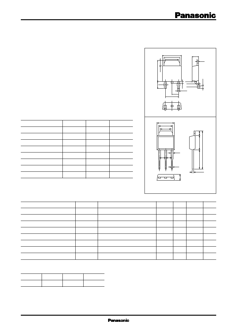
Unit: mm
1:Base
2:Collector
3:Emitter
U Type Package
6.5
▒
0.1
5.3
▒
0.1
4.35
▒
0.1
4.6
▒
0.1
2.3
▒
0.1
0.75
▒
0.1
1
2
3
0.93
▒
0.1
2.5
▒
0.1
0.8max
1.0
▒
0.2
7.3
▒
0.1
1.8
▒
0.1
2.3
▒
0.1
0.5
▒
0.1
0.5
▒
0.1
0.1
▒
0.05
1.0
▒
0.1
6.5
▒
0.2
2.3
5.35
4.35
13.3
▒
0.3
2.3
▒
0.1
5.5
▒
0.2
6.0
1.8
0.75
0.6
3
2.3
2
1
0.5
▒
0.1
1:Base
2:Collector
3:Emitter
EIAJ:SCş63
U Type Package (Z)
Unit: mm

2
Power Transistors
2SB967
P
C
-- Ta
I
C
-- V
CE
I
C
-- V
BE
V
CE(sat)
-- I
C
h
FE
-- I
C
f
T
-- I
E
C
ob
-- V
CB
0
160
40
120
80
140
20
100
60
0
32
24
8
20
28
16
4
12
T
C
=Ta
Ambient temperature Ta (░C)
Collector power dissipation P
C
(W
)
0
ş12
ş10
ş8
ş2
ş6
ş4
0
ş6
ş5
ş4
ş3
ş2
ş1
T
C
=25░C
ş35mA
ş25mA
ş30mA
ş20mA
ş15mA
ş10mA
ş1mA
ş5mA
I
B
=ş40mA
Collector to emitter voltage V
CE
(V)
Collector current I
C
(A
)
0
ş2.0
ş1.6
ş 0.4
ş1.2
ş 0.8
0
ş12
ş10
ş8
ş6
ş4
ş2
V
CE
=ş2V
T
C
=100░C
ş25░C
25░C
Base to emitter voltage V
BE
(V)
Collector current I
C
(A
)
ş 0.01
ş 0.1
ş1
ş10
ş 0.03
ş 0.3
ş3
ş 0.01
ş 0.03
ş 0.1
ş 0.3
ş1
ş3
ş10
ş30
ş100
I
C
/I
B
=30
25░C
T
C
=100░C
ş25░C
Collector current I
C
(A)
Collector to emitter saturation voltage V
CE(sat)
(V
)
ş 0.01
ş 0.1
ş1
ş10
ş 0.03
ş 0.3
ş3
10
30
100
300
1000
3000
10000
30000
100000
V
CE
=ş2V
T
C
=100░C
25░C
ş25░C
Collector current I
C
(A)
Forward current transfer ratio h
FE
1
3
10
30
100
0
240
200
160
120
80
40
V
CB
=ş6V
f=200MHz
T
C
=25░C
Emitter current I
E
(mA)
Transition frequency f
T
(MHz
)
ş1
ş3
ş10
ş30
ş100
0
200
160
120
80
40
I
E
=0
f=1MHz
T
C
=25░C
Collector to base voltage V
CB
(V)
Collector output capacitance C
ob
(pF
)