Low Noise, JFET Input
Operational Amplifiers
These low noise JFET input operational amplifiers combine two
stateoftheart analog technologies on a single monolithic integrated
circuit. Each internally compensated operational amplifier has well matched
high voltage JFET input device for low input offset voltage. The BIFET
technology provides wide bandwidths and fast slew rates with low input bias
currents, input offset currents, and supply currents. Moreover, the devices
exhibit low noise and low harmonic distortion, making them ideal for use in
high fidelity audio amplifier applications.
These devices are available in single, dual and quad operational
amplifiers which are pincompatible with the industry standard MC1741,
MC1458, and the MC3403/LM324 bipolar products.
·
Low Input Noise Voltage: 18 nV/ Hz Typ
·
Low Harmonic Distortion: 0.01% Typ
·
Low Input Bias and Offset Currents
·
High Input Impedance: 10
12
Typ
·
High Slew Rate: 13 V/
µ
s Typ
·
Wide Gain Bandwidth: 4.0 MHz Typ
·
Low Supply Current: 1.4 mA per Amp
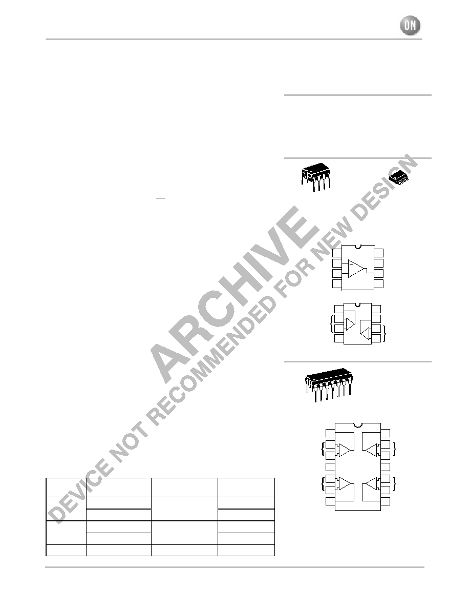
ORDERING INFORMATION
Op Amp
Function
Device
Operating
Temperature Range
Package
Single
TL071CD
T
0
°
to +70
°
C
SO8
Single
TL071ACP
T
A
= 0
°
to +70
°
C
Plastic DIP
Dual
TL072CD
T = 0
°
to +70
°
C
SO8
Dual
TL072ACP
T
A
= 0
°
to +70
°
C
Plastic DIP
Quad
TL074CN, ACN
T
A
= 0
°
to +70
°
C
Plastic DIP
ON Semiconductort
©
Semiconductor Components Industries, LLC, 2002
March, 2002 Rev. 2
1
Publication Order Number:
TL071C/D
TL071C,AC
TL072C,AC
TL074C,AC
SEMICONDUCTOR
TECHNICAL DATA
LOW NOISE, JFET INPUT
OPERATIONAL AMPLIFIERS
TL071 (Top View)
TL072 (Top View)
D SUFFIX
PLASTIC PACKAGE
CASE 751
(SO8)
P SUFFIX
PLASTIC PACKAGE
CASE 626
1
1
8
8
PIN CONNECTIONS
+
Offset Null
Noninvt Input
V
EE
Inv + Input
V
EE
Inputs A
Output A
NC
V
CC
Output
Offset Null
Inputs B
Output B
V
CC
+
+
1
8
7
6
5
2
3
4
1
8
7
6
5
2
3
4
TL074 (Top View)
N SUFFIX
PLASTIC PACKAGE
CASE 646
(TL074 Only)
PIN CONNECTIONS
4
2
3
1
14
1
Inputs 1
Output 1
V
CC
Inputs 2
Output 2
Output 4
Inputs 4
V
EE
Inputs 3
Output 3
+
+
+
+
1
14
13
12
11
10
9
8
2
3
4
5
6
7

TL071C,AC TL072C,AC TL074C,AC
http://onsemi.com
2
MAXIMUM RATINGS
Rating
Symbol
Value
Unit
Supply Voltage
V
CC
18
V
V
EE
18
Differential Input Voltage
V
ID
±
30
V
Input Voltage Range (Note 1)
V
IDR
±
15
V
Output Short Circuit Duration (Note 2)
t
SC
Continuous
Power Dissipation
Plastic Package (N, P)
P
D
680
mW
Derate above T
A
= 47
°
C
1.0/
JA
10
mW/
°
C
Operating Ambient Temperature Range
T
A
0 to +70
°
C
Storage Temperature Range
T
stg
65 to +150
°
C
NOTES: 1. The magnitude of the input voltage must not exceed the magnitude of the supply voltage or
15 V, whichever is less.
2. The output may be shorted to ground or either supply. Temperature and/or supply voltages
must be limited to ensure that power dissipation ratings are not exceeded.
3. ESD data available upon request.
ELECTRICAL CHARACTERISTICS
(V
CC
= 15 V, V
EE
= 15 V, T
A
= T
high
to T
low
[Note 1])
Characteristics
Symbol
Min
Typ
Max
Unit
Input Offset Voltage (R
S
10 k, V
CM
= 0)
V
IO
mV
TL071C, TL072C
13
TL074C
13
TL07_AC
7.5
Input Offset Current (V
CM
= 0) (Note 2)
I
IO
nA
TL07_C
2.0
TL07_AC
2.0
Input Bias Current (V
CM
= 0) (Note 2)
I
IB
nA
TL07_C
7.0
TL07_AC
7.0
LargeSignal Voltage Gain (V
O
=
±
10 V, R
L
2.0 k)
A
VOL
V/mV
TL07_C
15
TL07_AC
25
Output Voltage Swing (PeaktoPeak)
V
O
V
(R
L
10 k)
24
(R
L
2.0 k)
20
NOTES: 1. T
low
= 0
°
C for TL071C,AC
T
high
= 70
°
C for TL071C,AC
0
°
C for
TL072C,AC
T
high
= 70
°
C for
TL072C,AC
0
°
C for
TL074C,AC
T
high
= 70
°
C for
TL074C,AC
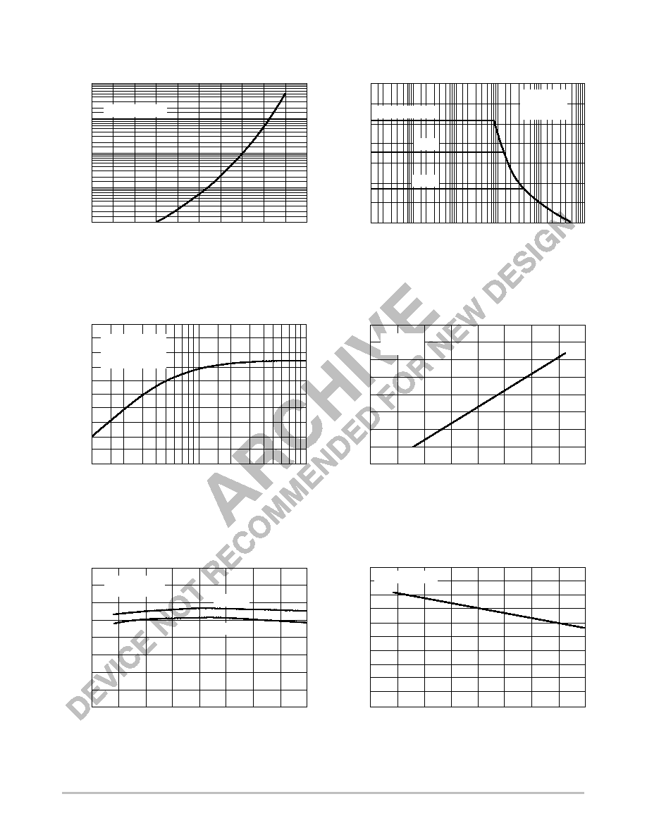
2. Input Bias currents of JFET input op amps approximately double for every 10
°
C rise in junction temperature as shown in Figure 3. To maintain
junction temperature as close to ambient temperature as possible, pulse techniques must be used during testing.
Figure 1. Unity Gain Voltage Follower
Figure 2. Inverting Gain of 10 Amplifier
-
+
V
in
R
L
= 2.0 k
V
O
C
L
= 100 pF
-
+
V
in
R
L
V
O
C
L
= 100 pF
10 k
1.0 k

TL071C,AC TL072C,AC TL074C,AC
http://onsemi.com
3
ELECTRICAL CHARACTERISTICS
(V
CC
= 15 V, V
EE
= 15 V, T
A
= 25
°
C, unless otherwise noted.)
Characteristics
Symbol
Min
Typ
Max
Unit
Input Offset Voltage (R
S
10 k, V
CM
= 0)
V
IO
mV
TL071C, TL072C
3.0
10
TL074C
3.0
10
TL07_AC
3.0
6.0
Average Temperature Coefficient of Input Offset Voltage
V
IO
/
T
10
µ
V/
°
C
R
S
= 50
, T
A
= T
low
to T
high
(Note 1)
Input Offset Current (V
CM =
0) (Note 2)
I
IO
pA
TL07_C
5.0
50
TL07_AC
5.0
50
Input Bias Current (V
CM
= 0) (Note 2)
I
IB
pA
TL07_C
30
200
TL07_AC
30
200
Input Resistance
r
i
10
12
Common Mode Input Voltage Range
V
ICR
V
TL07_C
±
10
15, 12
TL07_AC
±
11
15, 12
LargeSignal Voltage Gain (V
O
=
±
10 V, R
L
2.0 k)
A
VOL
V/mV
TL07_C
25
150
TL07_AC
50
150
Output Voltage Swing (PeaktoPeak)
V
O
24
28
V
(R
L
= 10 k)
Common Mode Rejection Ratio (R
S
10 k)
CMRR
dB
TL07_C
70
100
TL07_AC
80
100
Supply Voltage Rejection Ratio (R
S
10 k)
PSRR
dB
TL07_C
70
100
TL07_AC
80
100
Supply Current (Each Amplifier)
I
D
1.4
2.5
mA
Unity Gain Bandwidth
BW
4.0
MHz
Slew Rate (See Figure 1)
SR
13
v/
µ
s
V
in
= 10 V, R
L
= 2.0 k, C
L
= 100 pF
Rise Time (See Figure 1)
t
r
0.1
µ
s
Overshoot (V
in
= 20 mV, R
L
= 2.0 k, C
L
= 100 pF)
OS
10
%
Equivalent Input Noise Voltage
e
n
18
nV/ Hz
R
S
= 100
, f = 1000 Hz
Equivalent Input Noise Current
i
n
0.01
pA/ Hz
R
S
= 100
, f = 1000 Hz
Total Harmonic Distortion
THD
0.01
%
V
O
(RMS) = 10 V, R
S
1.0 k, R
L
2.0 k, f = 1000 Hz
Channel Separation
CS
120
dB
A
V
= 100
NOTES: 1. T
low
= 0
°
C for TL071C,AC
T
high
= 70
°
C for TL071C,AC
0
°
C for
TL072C,AC
T
high
= 70
°
C for
TL072C,AC
0
°
C for
TL074C,AC
T
high
= 70
°
C for
TL074C,AC
2. Input Bias currents of JFET input op amps approximately double for every 10
°
C rise in junction temperature as shown in Figure 3. To maintain
junction temperature as close to ambient temperature as possible, pulse techniques must be used during testing.
TL071C,AC TL072C,AC TL074C,AC
http://onsemi.com
4
V O
, OUTPUT
VOL
T
AGE SWING (V
pp
)
V O
, OUTPUT
VOL
T
AGE SWING (V
pp
)
V O
, OUTPUT
VOL
T
AGE SWING (V
pp
)
V O
, OUTPUT
VOL
T
AGE SWING (V
pp
)
V
CC
/V
EE
=
±
15 V
(See Figure 2)
R
L
= 10 k
R
L
= 2.0 k
Figure 3. Input Bias Current
versus Temperature
Figure 4. Output Voltage Swing
versus Frequency
Figure 5. Output Voltage Swing
versus Load Resistance
Figure 6. Output Voltage Swing
versus Supply Voltage
Figure 7. Output Voltage Swing
versus Temperature
Figure 8. Supply Current per Amplifier
versus Temperature
T
A
, AMBIENT TEMPERATURE (
°
C)
IB
-75 -50 -25
0
25
50
75 100 125
V
CC
/V
EE
=
±
15 V
100
1.0 k
10 k
100 k
1.0 M
10 M
f, FREQUENCY (Hz)
R
L
, LOAD RESISTANCE (k
)
0.1
0.2
0.4
0.7 1.0
2.0
10
4.0
7.0
V
CC
, |V
EE
| , SUPPLY VOLTAGE (
±
V)
0
5.0
10
15
20
R
L
= 2.0 k
T
A
= 25
°
C
T
A
, AMBIENT TEMPERATURE (
°
C)
-50
-25
0
25
50
75
100
125
T
A
, AMBIENT TEMPERATURE (
°
C)
-50
-25
0
25
50
75
100
125
I D
V
CC
/V
EE
=
±
15 V
T
A
= 25
°
C
(See Figure 2)
0.6
100
10
1.0
0.1
0.01
30
25
20
15
10
5.0
0
30
20
10
5.0
0
40
30
20
10
0
35
30
25
20
15
10
5.0
0
2.0
1.8
1.6
1.4
1.2
1.0
0.8
0.4
0.2
0
V
CC
/V
EE
=
±
15 V
±
10 V
±
5.0 V
R
L
= 2.0 k
T
A
= 25
°
C
(See Figure 2)
V
CC
/V
EE
=
±
15 V
I
,
INPUT
BIAS CURRENT
(nA)
, SUPPL
Y
DRAIN CURRENT
(mA)
-100
150
35
40
40
-75
-75
TL071C,AC TL072C,AC TL074C,AC
http://onsemi.com
5
, VOL
T
AGE GAIN (V/mV)
VOLV
, EQUIV
ALENT
INPUT
NOISE VOL
T
AGE (
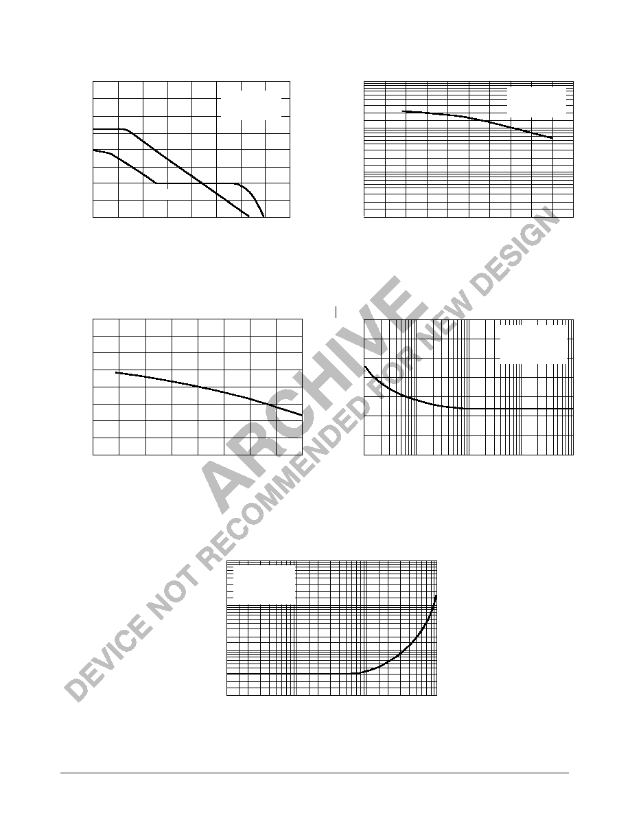
Figure 9. Large Signal Voltage Gain and
Phase Shift versus Frequency
Figure 10. Large Signal Voltage Gain
versus Temperature
Figure 11. Normalized Slew Rate
versus Temperature
Figure 12. Equivalent Input Noise Voltage
versus Frequency
Figure 13. Total Harmonic Distortion
versus Frequency
f, FREQUENCY (Hz)
PHASE SHIFT
(DEGREES)
10
6
10
5
10
4
10
3
10
1
10
2
1.0
1.0
10
100
1.0 k 10 k
100 k 1.0 M 10 M
, OPEN-LOOP
GAIN
VOL
Gain
Phase Shift
V
CC
/V
EE
=
±
15 V
R
L
= 2.0 k
T
A
= 25
°
C
V
CC
/V
EE
=
±
15 V
V
O
=
±
10 V
R
L
= 2.0 k
T
A
, AMBIENT TEMPERATURE (
°
C)
1000
100
10
1.0
-50 -25
0
25
50
75
100 125
T
A
, AMBIENT TEMPERATURE (
°
C)
NORMALIZED SLEW RA
TE
1.15
1.10
1.05
1.0
0.95
0.90
0.85
-50
-25
0
25
50
75
100
125
f, FREQUENCY (Hz)
60
50
40
30
20
10
0
0.01
0.05 0.1
0.5 1.0
5.0 10
50 100
V
CC
/V
EE
=
±
15 Vdc
A
V
= 10
R
S
= 100
T
A
= 25
°
C
V
CC
/V
EE
=
±
15 V
A
V
= 1.0
V
O
= 6.0 V (RMS)
T
A
= 25
°
C
f, FREQUENCY (Hz)
THD,
T
O
T
A
L
HARMONIC DIST
OR
TION (%)
1.0
0.5
0.1
0.05
0.01
0.005
0.001
0.1
0.5 1.0
5.0
10
50
100
0
°
45
°
90
°
135
°
180
°
V
e
nV/
Hz
n
)
10
7
10
8
100 M
-75
-100
150
1.20
0.80
-75
70