®
Semiconductor Components Industries, LLC, 2000
May, 2000 Ł Rev. 3
1
Publication Order Number:
T2322/D
T2322B
Sensitive Gate Triacs
Silicon Bidirectional Thyristors
Designed primarily for ac power switching. The gate sensitivity of
these triacs permits the use of economical transistorized or integrated
circuit control circuits, and it enhances their use in low-power phase
control and load-switching applications.
Ę
Very High Gate Sensitivity
Ę
Low On-State Voltage at High Current Levels
Ę
Glass-Passivated Chip for Stability
Ę
Small, Rugged Thermopad Construction for Low Thermal
Resistance, High Heat Dissipation and Durability
Ę
Device Marking: Device Type, e.g., T2322B, Date Code
MAXIMUM RATINGS
(TJ = 25
░
C unless otherwise noted)
Rating
Symbol
Value
Unit
Peak Repetitive Off-State Voltage(1)
(TJ = 25 to 110
░
C, Gate Open)
VDRM,
VRRM
200
Volts
On-State RMS Current (TC = 70
░
C)
(Full Cycle Sine Wave 50 to 60 Hz)
IT(RMS)
2.5
Amps
Peak NonŁRepetitive Surge Current
(One Full Cycle, Sine Wave 60 Hz,
TC = 70
░
C)
ITSM
25
Amps
Circuit Fusing Consideration
(t = 8.3 ms)
I2t
2.6
A2s
Peak Gate Power
(Pulse Width
10
Ą
s, TC = 70
░
C)
PGM
10
Watts
Average Gate Power
(t = 8.3 ms, TC = 70
░
C)
PG(AV)
0.5
Watt
Peak Gate Current
(Pulse Width = 10
Ą
s, TC = 70
░
C)
IGM
0.5
Amp
Operating Junction Temperature Range
TJ
Ł40 to
+110
░
C
Storage Temperature Range
Tstg
Ł40 to
+150
░
C
Mounting Torque (6-32 Screw)(2)
--
8.0
in. lb.
(1) VDRM and VRRM for all types can be applied on a continuous basis. Blocking
voltages shall not be tested with a constant current source such that the
voltage ratings of the devices are exceeded.
(2) Torque rating applies with use of torque washer (Shakeproof WD19523 or
equivalent). Mounting Torque in excess of 6 in. lb. does not appreciably
lower case-to-sink thermal resistance. Main terminal 2 and heat-sink
contact pad are common.
TRIACS
2.5 AMPERES RMS
200 VOLTS
Device
Package
Shipping
ORDERING INFORMATION
T2322B
TO225AA
500/Box
http://onsemi.com
TOŁ225AA
(formerly TOŁ126)
CASE 077
STYLE 5
1
2
3
PIN ASSIGNMENT
1
2
3
Main Terminal 2
Gate
Main Terminal 1
MT1
G
MT2

T2322B
http://onsemi.com
2
THERMAL CHARACTERISTICS
Characteristic
Symbol
Max
Unit
Thermal Resistance, Junction to Case
R
JC
3.5
░
C/W
Thermal Resistance, Junction to Ambient
R
JA
60
░
C/W
Maximum Lead Temperature for Soldering Purposes 1/8
from Case for 10 Seconds
TL
260
░
C
ELECTRICAL CHARACTERISTICS
(TC = 25
░
C unless otherwise noted; Electricals apply in both directions)
Characteristic
Symbol
Min
Typ
Max
Unit
OFF CHARACTERISTICS
Peak Repetitive Blocking Current
(VD = Rated VDRM, VRRM; Gate Open)
TJ = 25
░
C
TJ = 110
░
C
IDRM,
IRRM
--
--
--
0.2
10
0.75
Ą
A
mA
ON CHARACTERISTICS
Peak On-State Voltage(1)
(ITM =
"
10 A)
VTM
--
1.7
2.2
Volts
Gate Trigger Current (Continuous dc)
(VD = 12 V, RL = 100
)
All Quadrants
IGT
--
--
10
mA
Gate Trigger Voltage (Continuous dc)
(VD = 12 Vdc, RL = 100
, TC = 25
░
C)
VGT
--
1.0
2.2
Volts
Gate NonŁTrigger Voltage
(VD = 12 V, RL = 100
, TC = 110
░
C)
VGD
0.15
--
--
Volts
Holding Current
(VD = 12 V, IT (Initiating Current) =
"
200 mA, Gate Open)
IH
--
15
30
mA
Gate Controlled Turn-On Time
(VD = Rated VDRM, ITM = 10 A pk, IG = 60 mA, tr = 0.1
Ą
sec)
tgt
--
1.8
2.5
Ą
s
DYNAMIC CHARACTERISTICS
Critical Rate-of-Rise of Off-State Voltage
(VD = Rated VDRM, Exponential Waveform, TC = 100
░
C)
dv/dt
10
100
--
V/
Ą
s
Critical Rate-of-Rise of Commutation Voltage
(VD = Rated VDRM, ITM = 3.5 A pk, Commutating
di/dt = 1.26 A/ms, Gate Unenergized, TC = 90
░
C)
dv/dt(c)
1.0
4.0
--
V/
Ą
s
(1) Pulse Test: Pulse Width
1.0 ms, Duty Cycle
2%.
T2322B
http://onsemi.com
3
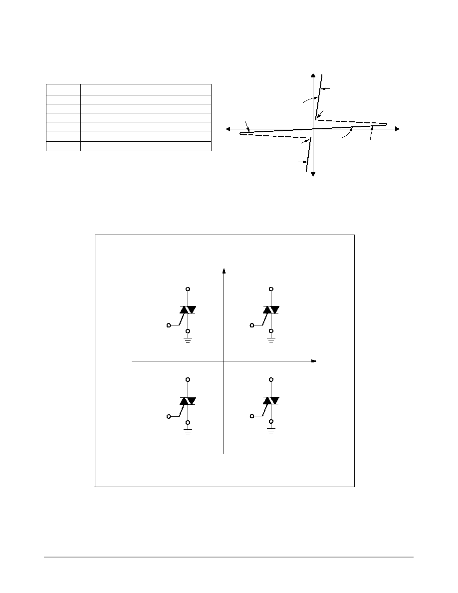
+ Current
+ Voltage
VTM
IH
Symbol
Parameter
VDRM
Peak Repetitive Forward Off State Voltage
IDRM
Peak Forward Blocking Current
VRRM
Peak Repetitive Reverse Off State Voltage
IRRM
Peak Reverse Blocking Current
Voltage Current Characteristic of Triacs
(Bidirectional Device)
IDRM at VDRM
on state
off state
IRRM at VRRM
Quadrant 1
MainTerminal 2 +
Quadrant 3
MainTerminal 2 Ł
VTM
IH
VTM
Maximum On State Voltage
IH
Holding Current
MT1
(+) IGT
GATE
(+) MT2
REF
MT1
(Ł) IGT
GATE
(+) MT2
REF
MT1
(+) IGT
GATE
(Ł) MT2
REF
MT1
(Ł) IGT
GATE
(Ł) MT2
REF
Ł
MT2 NEGATIVE
(Negative Half Cycle)
MT2 POSITIVE
(Positive Half Cycle)
+
Quadrant III
Quadrant IV
Quadrant II
Quadrant I
Quadrant Definitions for a Triac
IGT Ł
+ IGT
All polarities are referenced to MT1.
With inŁphase signals (using standard AC lines) quadrants I and III are used.
T2322B
http://onsemi.com
4
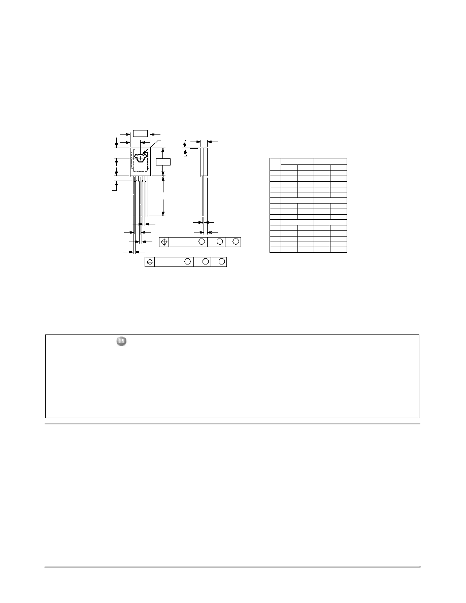
PACKAGE DIMENSIONS
NOTES:
1. DIMENSIONING AND TOLERANCING PER ANSI
Y14.5M, 1982.
2. CONTROLLING DIMENSION: INCH.
ŁBŁ
ŁAŁ
M
K
F
C
Q
H
V
G
S
D
J
R
U
1
3
2
2 PL
M
A
M
0.25 (0.010)
B
M
M
A
M
0.25 (0.010)
B
M
DIM
MIN
MAX
MIN
MAX
MILLIMETERS
INCHES
A
0.425
0.435
10.80
11.04
B
0.295
0.305
7.50
7.74
C
0.095
0.105
2.42
2.66
D
0.020
0.026
0.51
0.66
F
0.115
0.130
2.93
3.30
G
0.094 BSC
2.39 BSC
H
0.050
0.095
1.27
2.41
J
0.015
0.025
0.39
0.63
K
0.575
0.655
14.61
16.63
M
5 TYP
5 TYP
Q
0.148
0.158
3.76
4.01
R
0.045
0.065
1.15
1.65
S
0.025
0.035
0.64
0.88
U
0.145
0.155
3.69
3.93
V
0.040
ŁŁŁ
1.02
ŁŁŁ
_
_
STYLE 5:
PIN 1. MT 1
2. MT 2
3. GATE
TOŁ225AA
(formerly TOŁ126)
CASE 077Ł09
ISSUE W
ON Semiconductor and are trademarks of Semiconductor Components Industries, LLC (SCILLC). SCILLC reserves the right to make changes
without further notice to any products herein. SCILLC makes no warranty, representation or guarantee regarding the suitability of its products for any particular
purpose, nor does SCILLC assume any liability arising out of the application or use of any product or circuit, and specifically disclaims any and all liability,
including without limitation special, consequential or incidental damages. "Typical" parameters which may be provided in SCILLC data sheets and/or
specifications can and do vary in different applications and actual performance may vary over time. All operating parameters, including "Typicals" must be
validated for each customer application by customer's technical experts. SCILLC does not convey any license under its patent rights nor the rights of others.
SCILLC products are not designed, intended, or authorized for use as components in systems intended for surgical implant into the body, or other applications
intended to support or sustain life, or for any other application in which the failure of the SCILLC product could create a situation where personal injury or
death may occur. Should Buyer purchase or use SCILLC products for any such unintended or unauthorized application, Buyer shall indemnify and hold
SCILLC and its officers, employees, subsidiaries, affiliates, and distributors harmless against all claims, costs, damages, and expenses, and reasonable
attorney fees arising out of, directly or indirectly, any claim of personal injury or death associated with such unintended or unauthorized use, even if such claim
alleges that SCILLC was negligent regarding the design or manufacture of the part. SCILLC is an Equal Opportunity/Affirmative Action Employer.
PUBLICATION ORDERING INFORMATION
CENTRAL/SOUTH AMERICA:
Spanish Phone: 303Ł308Ł7143 (MonŁFri 8:00am to 5:00pm MST)
Email: ONlitŁspanish@hibbertco.com
ASIA/PACIFIC: LDC for ON Semiconductor Ł Asia Support
Phone: 303Ł675Ł2121 (TueŁFri 9:00am to 1:00pm, Hong Kong Time)
Toll Free from Hong Kong & Singapore:
001Ł800Ł4422Ł3781
Email: ONlitŁasia@hibbertco.com
JAPAN: ON Semiconductor, Japan Customer Focus Center
4Ł32Ł1 NishiŁGotanda, ShinagawaŁku, Tokyo, Japan 141Ł0031
Phone: 81Ł3Ł5740Ł2745
Email: r14525@onsemi.com
ON Semiconductor Website: http://onsemi.com
For additional information, please contact your local
Sales Representative.
T2322/D
NORTH AMERICA Literature Fulfillment:
Literature Distribution Center for ON Semiconductor
P.O. Box 5163, Denver, Colorado 80217 USA
Phone: 303Ł675Ł2175 or 800Ł344Ł3860 Toll Free USA/Canada
Fax: 303Ł675Ł2176 or 800Ł344Ł3867 Toll Free USA/Canada
Email: ONlit@hibbertco.com
Fax Response Line: 303Ł675Ł2167 or 800Ł344Ł3810 Toll Free USA/Canada
N. American Technical Support: 800Ł282Ł9855 Toll Free USA/Canada
EUROPE: LDC for ON Semiconductor Ł European Support
German Phone: (+1) 303Ł308Ł7140 (MŁF 1:00pm to 5:00pm Munich Time)
Email: ONlitŁgerman@hibbertco.com
French Phone: (+1) 303Ł308Ł7141 (MŁF 1:00pm to 5:00pm Toulouse Time)
Email: ONlitŁfrench@hibbertco.com
English Phone: (+1) 303Ł308Ł7142 (MŁF 12:00pm to 5:00pm UK Time)
Email: ONlit@hibbertco.com
EUROPEAN TOLLŁFREE ACCESS*: 00Ł800Ł4422Ł3781
*Available from Germany, France, Italy, England, Ireland