©
Semiconductor Components Industries, LLC, 2002
April, 2002 Rev. 5
1
Publication Order Number:
SMS05T1/D
SMS05T1 Series
SC-74 Quad Transient
Voltage Suppressor
for ESD Protection
This quad monolithic silicon voltage suppressor is designed for
applications requiring transient overvoltage protection capability. It is
intended for use in voltage and ESD sensitive equipment such as
computers, printers, business machines, communication systems and
other applications. This quad device provides superior surge
protection over current quad Zener MMQA series by providing up to
350 watts peak power.
Features:
·
SC-74 Package Allows Four Separate Unidirectional Configurations
·
Peak Power 350 Watts, 8 x 20
mS
·
ESD Rating of Class N (Exceeding 25 kV) per the
Human Body Model
·
ESD Rating:
IEC 6100042 (ESD) 15 kV (air) 8 kV (contact)
IEC 6100044 (EFT) 40 Amps (5/50 ns)
IEC 6100045 (lightning) 23 Amps (8/20
ms)
·
UL Flammability Rating of 94V0
Typical Applications:
·
Hand Held Portable Applications such as Cell Phones, Pagers,
Notebooks and Notebook Computers
MAXIMUM RATINGS
Rating
Symbol
Value
Unit
Peak Power Dissipation
8 x 20
m
S @ T
A
= 25
°
C (Note 1)
P
pk
350
W
Total Power Dissipation on FR5 Board
@ T
A
= 25
°
C (Note 2)
Derate Above 25
°
C
P
D
225
1.8
mW
mW/
°
C
Thermal Resistance,
JunctiontoAmbient
R
q
JA
556
°
C/W
Junction and Storage
Temperature Range
T
J
, T
stg
55 to
+150
°
C
Lead Solder Temperature
Maximum 10 Seconds Duration
T
L
260
°
C
1. Nonrepetitive current pulse 8 x 20
m
S exponential decay waveform
2. FR5 = 1.0 x 0.75 x 0.62 in.
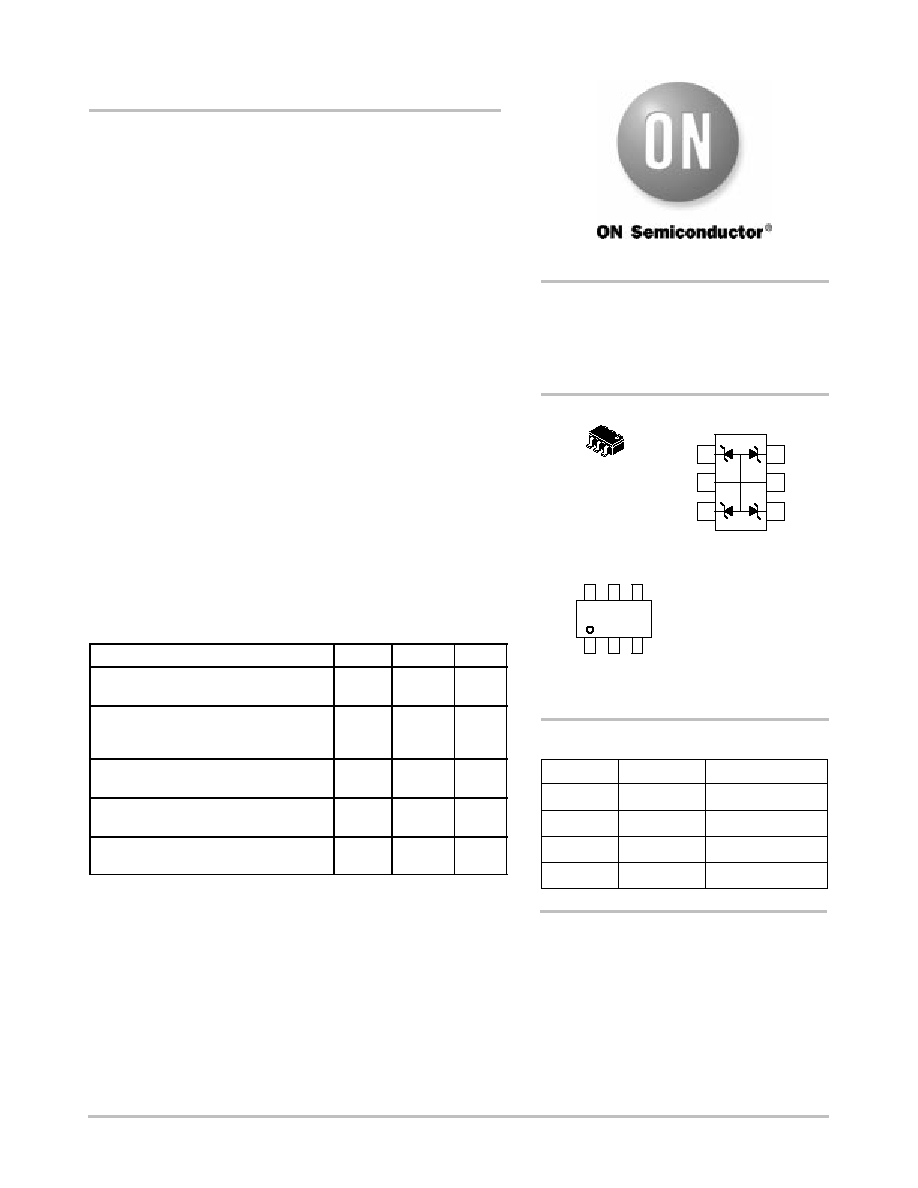
SC74 QUAD TRANSIENT
VOLTAGE SUPPRESSOR
350 WATTS PEAK POWER
5 VOLTS
SC74
CASE 318F
STYLE 1
1
2
3
4
5 6
1
2
3
6
5
4
xxx
= Device Code
d
= Date Code
MARKING
DIAGRAM
PIN ASSIGNMENT
Device
Package
Shipping
ORDERING INFORMATION
SMS05T1
SC74
3000/Tape & Reel
xxx
d
PIN 1. CATHODE
2. ANODE
3. CATHODE
4. CATHODE
5. ANODE
6. CATHODE
See specific marking information in the device marking
column of the Electrical Characteristics table on page 2 of
this data sheet.
DEVICE MARKING INFORMATION
SMS12T1
SC74
3000/Tape & Reel
SMS15T1
SC74
3000/Tape & Reel
SMS24T1
SC74
3000/Tape & Reel
http://onsemi.com
SMS05T1 Series
http://onsemi.com
2
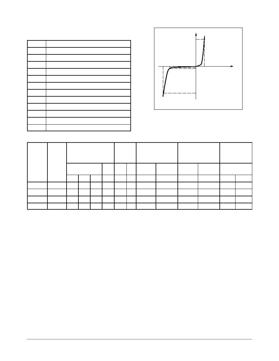
ELECTRICAL CHARACTERISTICS
(T
A
= 25
°
C unless otherwise noted)
Symbol
Parameter
I
PP
Maximum Reverse Peak Pulse Current
V
C
Clamping Voltage @ I
PP
V
RWM
Working Peak Reverse Voltage
I
R
Maximum Reverse Leakage Current @ V
RWM
V
BR
Breakdown Voltage @ I
T
I
T
Test Current
Q
V
BR
Maximum Temperature Coefficient of V
BR
I
F
Forward Current
V
F
Forward Voltage @ I
F
Z
ZT
Maximum Zener Impedance @ I
ZT
I
ZK
Reverse Current
Z
ZK
Maximum Zener Impedance @ I
ZK
UniDirectional
I
PP
I
F
V
I
I
R
I
T
V
RWM
V
C
V
BR
V
F
ELECTRICAL CHARACTERISTICS UNIDIRECTIONAL
Breakdown
Voltage
Max
Reverse
Leakage
Current
Max Reverse Voltage
(Clamping Voltage)
At Specified Reverse
Surge Current (I
RSM
)
Max Reverse Voltage
(Clamping Voltage)
At Specified Reverse
Surge Current (I
RSM
)
Capacitance
@ 0 Volt Bias,
1 MHz
Device
V
BR
(V)
I
T
I
R
V
R
I
RSM
(8x20
m
s)
V
RSM
(8x20
m
s)
I
RSM
(8x20
m
s)
V
RSM
(8x20
m
s)
(pF)
Device
Device
Marking
Min
Nom
Max
(mA)
(
m
A)
(V)
(A)
(V)
(A)
(V)
Min
Max
SMS05T1
5V0
6.0
7.2
1.0
20
5.0
5.0
9.8
23
15.5
250
400
SMS12T1
12V
13.3
15
1.0
1.0
12
5.0
19.0
15
23.0
80
150
SMS15T1
15V
16.7
18.5
1.0
1.0
15
5.0
24.0
12
29.0
60
125
SMS24T1
24V
26.7
32
1.0
1.0
24
5.0
40.0
8
44.0
40
75
SMS05T1 Series
http://onsemi.com
3
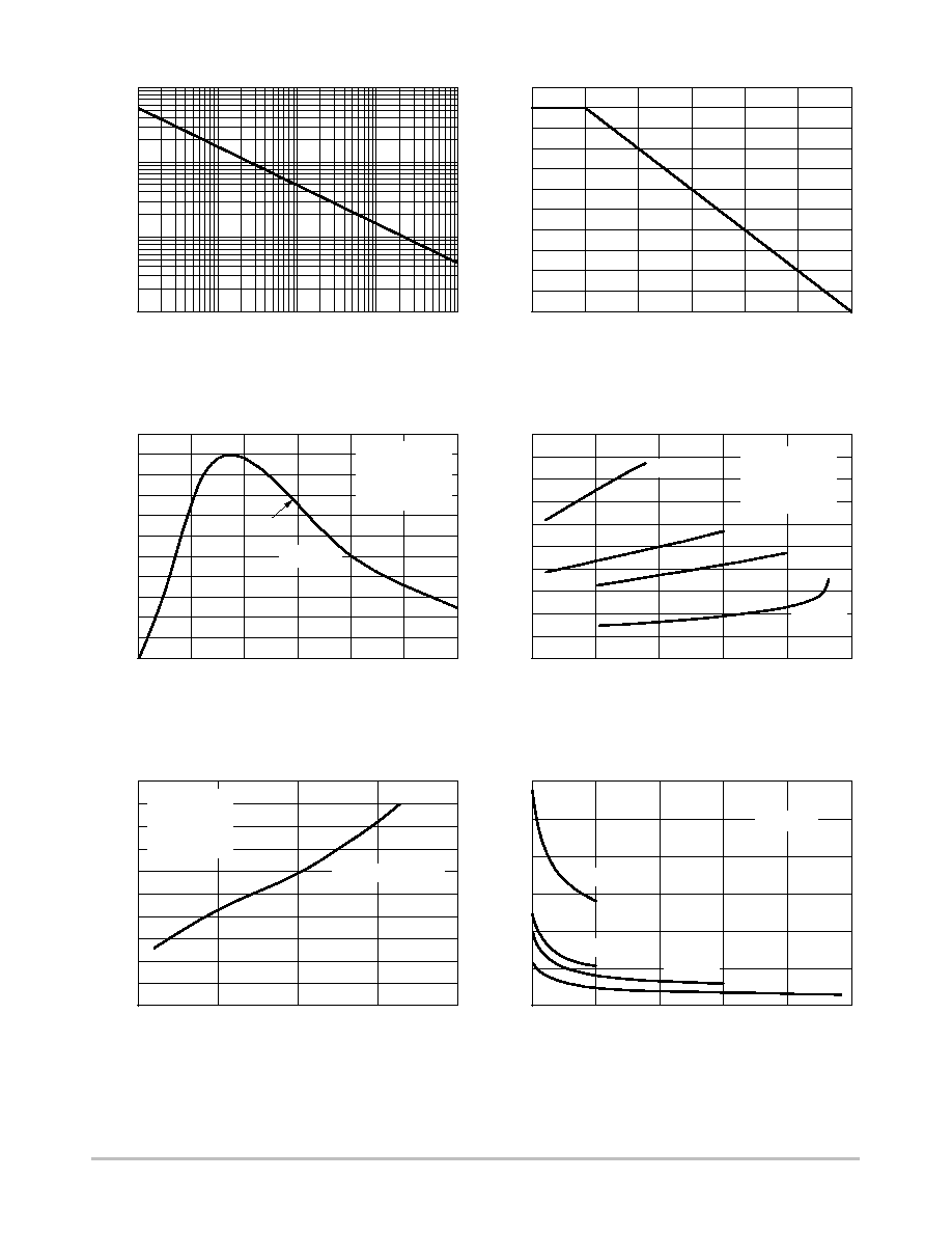
SMS15
SMS12
Figure 1. NonRepetitive Peak Pulse Power
versus Pulse Time
Figure 2. Power Derating Curve
Figure 3. Pulse Waveform
t, TIME (
m
s)
30
15
10
5
0
Figure 4. Clamping Voltage versus
Peak Pulse Current
I
PP
, PEAK PULSE CURRENT (A)
25
20
15
10
5
0
15
10
5
0
25
PERCENT OF I
PP
V
C
, CLAMPING VOL
T
AGE (V)
Figure 5. 8 x 20
m
s V
F
I
F
, FORWARD CURRENT (A)
5
3
1
10
5
0
Figure 6. Typical Capacitance (SMS05 Series)
V
R
, REVERSE VOLTAGE (V)
25
20
15
10
5
0
150
100
50
0
0
200
250
V
F
, FOR
W
ARD VOL
T
AGE (V)
C, CAP
ACIT
ANCE (pF)
25
20
90
80
70
60
50
40
30
20
10
0
100
110
WAVEFORM
PARAMETERS
t
r
= 8
m
s
t
d
= 20
m
s
t
d
= I
PP
/2
4
20
15
PULSE
WAVEFORM
t
r
= 8
m
s
t
d
= 20
m
s
WAVEFORM
PARAMETERS
t
r
= 8
m
s
t
d
= 20
m
s
20
SMS24
2
300
T
J
= 25
°
C
ct
8 X 20
m
s SURGE
SMS05
SMS12
SMS05
t
p
, PULSE DURATION (
m
s)
10
1
0.1
1000
100
10
1
0.1
T
A
, AMBIENT TEMPERATURE (
°
C)
150
125
100
75
50
25
0
90
80
70
60
50
40
30
20
10
0
0.01
100
110
P
PP
, PEAK PULSE POWER (kW)
% OF RA
TED POWER OR I
PP
SMS15
SMS24
40
35
30
50
45
SMS05T1 Series
http://onsemi.com
4
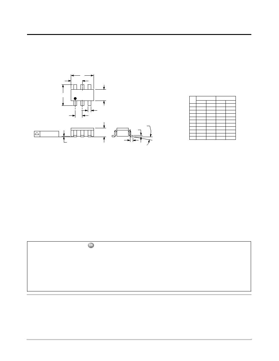
350 Watts Peak Power
Transient Voltage Suppressors Surface Mount
SC74 (SC59ML)
CASE 318F03
ISSUE F
STYLE 1:
PIN 1. CATHODE
2. ANODE
3. CATHODE
4. CATHODE
5. ANODE
6. CATHODE
2
3
4
5
6
A
L
1
S
G
D
B
H
C
0.05 (0.002)
DIM
MIN
MAX
MIN
MAX
MILLIMETERS
INCHES
A 0.1142 0.1220
2.90
3.10
B 0.0512 0.0669
1.30
1.70
C 0.0354 0.0433
0.90
1.10
D 0.0098 0.0197
0.25
0.50
G 0.0335 0.0413
0.85
1.05
H 0.0005 0.0040
0.013
0.100
J 0.0040 0.0102
0.10
0.26
K 0.0079 0.0236
0.20
0.60
L 0.0493 0.0649
1.25
1.65
M
0
10
0
10
S 0.0985 0.1181
2.50
3.00
_
_
_
_
NOTES:
1. DIMENSIONING AND TOLERANCING PER ANSI
Y14.5M, 1982.
2. CONTROLLING DIMENSION: INCH.
3. MAXIMUM LEAD THICKNESS INCLUDES LEAD
FINISH THICKNESS. MINIMUM LEAD THICKNESS
IS THE MINIMUM THICKNESS OF BASE
MATERIAL.
4. 318F-01 AND -02 OBSOLETE. NEW STANDARD
318F-03.
M
J
K
ON Semiconductor is a trademark and is a registered trademark of Semiconductor Components Industries, LLC (SCILLC). SCILLC reserves the right
to make changes without further notice to any products herein. SCILLC makes no warranty, representation or guarantee regarding the suitability of its products
for any particular purpose, nor does SCILLC assume any liability arising out of the application or use of any product or circuit, and specifically disclaims any
and all liability, including without limitation special, consequential or incidental damages. "Typical" parameters which may be provided in SCILLC data sheets
and/or specifications can and do vary in different applications and actual performance may vary over time. All operating parameters, including "Typicals" must
be validated for each customer application by customer's technical experts. SCILLC does not convey any license under its patent rights nor the rights of others.
SCILLC products are not designed, intended, or authorized for use as components in systems intended for surgical implant into the body, or other applications
intended to support or sustain life, or for any other application in which the failure of the SCILLC product could create a situation where personal injury or death
may occur. Should Buyer purchase or use SCILLC products for any such unintended or unauthorized application, Buyer shall indemnify and hold SCILLC
and its officers, employees, subsidiaries, affiliates, and distributors harmless against all claims, costs, damages, and expenses, and reasonable attorney fees
arising out of, directly or indirectly, any claim of personal injury or death associated with such unintended or unauthorized use, even if such claim alleges that
SCILLC was negligent regarding the design or manufacture of the part. SCILLC is an Equal Opportunity/Affirmative Action Employer.
PUBLICATION ORDERING INFORMATION
JAPAN: ON Semiconductor, Japan Customer Focus Center
4321 NishiGotanda, Shinagawaku, Tokyo, Japan 1410031
Phone: 81357402700
Email: r14525@onsemi.com
ON Semiconductor Website: http://onsemi.com
For additional information, please contact your local
Sales Representative.
SMS05T1/D
Literature Fulfillment:
Literature Distribution Center for ON Semiconductor
P.O. Box 5163, Denver, Colorado 80217 USA
Phone: 3036752175 or 8003443860 Toll Free USA/Canada
Fax: 3036752176 or 8003443867 Toll Free USA/Canada
Email: ONlit@hibbertco.com
N. American Technical Support: 8002829855 Toll Free USA/Canada