©
Semiconductor Components Industries, LLC, 2000
November, 2000 Rev. 0
1
Publication Order Number:
PN2222/D
PN2222, PN2222A
PN2222A is a Preferred Device
General Purpose
Transistors
NPN Silicon
MAXIMUM RATINGS
Rating
Symbol
Value
Unit
Collector-Emitter Voltage
PN2222
PN2222A
V
CEO
30
40
Vdc
Collector-Base Voltage
PN2222
PN2222A
V
CBO
60
75
Vdc
Emitter-Base Voltage
PN2222
PN2222A
V
EBO
5.0
6.0
Vdc
Collector Current Continuous
I
C
600
mAdc
Total Device Dissipation
@ T
A
= 25
°
C
Derate above 25
°
C
P
D
625
5.0
mW
mW/
°
C
Total Device Dissipation
@ T
C
= 25
°
C
Derate above 25
°
C
P
D
1.5
12
Watts
mW/
°
C
Operating and Storage Junction
Temperature Range
T
J
, T
stg
55 to
+150
°
C
THERMAL CHARACTERISTICS
Characteristic
Symbol
Max
Unit
Thermal Resistance
Junction-to-Ambient
R
JA
200
°
C/W
Thermal Resistance
Junction-to-Case
R
JC
83.3
°
C/W
Device
Package
Shipping
ORDERING INFORMATION
TO92
CASE 29
STYLE 1
http://onsemi.com
PN2222
TO92
5000 Units/Box
MARKING DIAGRAM
PN
222x
YWW
PN222x= Device Code
x
= 2 or A
Y
= Year
WW
= Work Week
Preferred devices are recommended choices for future use
and best overall value.
COLLECTOR
3
2
BASE
1
EMITTER
1
2
3
PN2222A
TO92
5000 Units/Box
PN2222ARLRA
TO92
2000/Tape & Reel
PN2222ARLRM
TO92
2000/Ammo Pack
PN2222ARLRP
TO92
2000/Ammo Pack

PN2222, PN2222A
http://onsemi.com
2
ELECTRICAL CHARACTERISTICS
(T
A
= 25
°
C unless otherwise noted)
Characteristic
Symbol
Min
Max
Unit
OFF CHARACTERISTICS
CollectorEmitter Breakdown Voltage
PN2222
(I
C
= 10 mAdc, I
B
= 0)
PN2222A
V
(BR)CEO
30
40
Vdc
CollectorBase Breakdown Voltage
PN2222
(I
C
= 10
m
Adc, I
E
= 0)
PN2222A
V
(BR)CBO
60
75
Vdc
EmitterBase Breakdown Voltage
PN2222
(I
E
= 10
m
Adc, I
C
= 0)
PN2222A
V
(BR)EBO
5.0
6.0
Vdc
Collector Cutoff Current
(V
CE
= 60 Vdc, V
EB(off)
= 3.0 Vdc)
PN2222A
I
CEX
10
nAdc
Collector Cutoff Current
(V
CB
= 50 Vdc, I
E
= 0)
PN2222
(V
CB
= 60 Vdc, I
E
= 0)
PN2222A
(V
CB
= 50 Vdc, I
E
= 0, T
A
= 125
°
C)
PN2222
(V
CB
= 50 Vdc, I
E
= 0, T
A
= 125
°
C)
PN2222A
I
CBO
0.01
0.01
10
10
µ
Adc
Emitter Cutoff Current
(V
EB
= 3.0 Vdc, I
C
= 0)
PN2222A
I
EBO
100
nAdc
Base Cutoff Current
(V
CE
= 60 Vdc, V
EB(off)
= 3.0 Vdc)
PN2222A
I
BL
20
nAdc
ON CHARACTERISTICS
DC Current Gain
(I
C
= 0.1 mAdc, V
CE
= 10 Vdc)
(I
C
= 1.0 mAdc, V
CE
= 10 Vdc)
(I
C
= 10 mAdc, V
CE
= 10 Vdc)
(I
C
= 10 mAdc, V
CE
= 10 Vdc, T
A
= 55
°
C)
PN2222A only
(I
C
= 150 mAdc, V
CE
= 10 Vdc) (Note 1.)
(I
C
= 150 mAdc, V
CE
= 1.0 Vdc) (Note 1.)
(I
C
= 500 mAdc, V
CE
= 10 Vdc) (Note 1.)
PN2222
PN2222A
h
FE
35
50
75
35
100
50
30
40
300
CollectorEmitter Saturation Voltage (Note 1.)
(I
C
= 150 mAdc, I
B
= 15 mAdc)
PN2222
PN2222A
(I
C
= 500 mAdc, I
B
= 50 mAdc)
PN2222
PN2222A
V
CE(sat)
0.4
0.3
1.6
1.0
Vdc
BaseEmitter Saturation Voltage (Note 1.)
(I
C
= 150 mAdc, I
B
= 15 mAdc)
PN2222
PN2222A
(I
C
= 500 mAdc, I
B
= 50 mAdc)
PN2222
PN2222A
V
BE(sat)
0.6
1.3
1.2
2.6
2.0
Vdc
1. Pulse Test: Pulse Width
v
300
m
s, Duty Cycle
v
2.0%.
PN2222, PN2222A
http://onsemi.com
3
ELECTRICAL CHARACTERISTICS
(T
A
= 25
°
C unless otherwise noted) (Continued)
Characteristic
Symbol
Min
Max
Unit
SMALLSIGNAL CHARACTERISTICS
CurrentGain Bandwidth Product (Note 2.)
(I
C
= 20 mAdc, V
CE
= 20 Vdc, f = 100 MHz)
PN2222
PN2222A
f
T
250
300
MHz
Output Capacitance
(V
CB
= 10 Vdc, I
E
= 0, f = 1.0 MHz)
C
obo
8.0
pF
Input Capacitance
(V
EB
= 0.5 Vdc, I
C
= 0, f = 1.0 MHz)
PN2222
PN2222A
C
ibo
30
25
pF
Input Impedance
(I
C
= 1.0 mAdc, V
CE
= 10 Vdc, f = 1.0 kHz)
PN2222A
(I
C
= 10 mAdc, V
CE
= 10 Vdc, f = 1.0 kHz)
PN2222A
h
ie
2.0
0.25
8.0
1.25
k
Voltage Feedback Ratio
(I
C
= 1.0 mAdc, V
CE
= 10 Vdc, f = 1.0 kHz)
PN2222A
(I
C
= 10 mAdc, V
CE
= 10 Vdc, f = 1.0 kHz)
PN2222A
h
re
8.0
4.0
X 10
4
SmallSignal Current Gain
(I
C
= 1.0 mAdc, V
CE
= 10 Vdc, f = 1.0 kHz)
PN2222A
(I
C
= 10 mAdc, V
CE
= 10 Vdc, f = 1.0 kHz)
PN2222A
h
fe
50
75
300
375
Output Admittance
(I
C
= 1.0 mAdc, V
CE
= 10 Vdc, f = 1.0 kHz)
PN2222A
(I
C
= 10 mAdc, V
CE
= 10 Vdc, f = 1.0 kHz)
PN2222A
h
oe
5.0
25
35
200
m
mhos
Collector Base Time Constant
(I
E
= 20 mAdc, V
CB
= 20 Vdc, f = 31.8 MHz)
PN2222A
rb
C
c
150
ps
Noise Figure
(I
C
= 100
m
Adc, V
CE
= 10 Vdc, R
S
= 1.0 k
, f = 1.0 kHz)
PN2222A
NF
4.0
dB
SWITCHING CHARACTERISTICS PN2222A only
Delay Time
(V
CC
= 30 Vdc, V
BE(off)
= 0.5 Vdc,
t
d
10
ns
Rise Time
(V
CC
30 Vdc, V
BE(off)
0.5 Vdc,
I
C
= 150 mAdc, I
B1
= 15 mAdc) (Figure 1)
t
r
25
ns
Storage Time
(V
CC
= 30 Vdc, I
C
= 150 mAdc,
t
s
225
ns
Fall Time
(V
CC
30 Vdc, I
C
150 mAdc,
I
B1
= I
B2
= 15 mAdc) (Figure 2)
t
f
60
ns
2. f
T
is defined as the frequency at which |h
fe
| extrapolates to unity.
Figure 1. TurnOn Time
Figure 2. TurnOff Time
SWITCHING TIME EQUIVALENT TEST CIRCUITS
Scope rise time < 4 ns
*Total shunt capacitance of test jig, connectors, and oscilloscope.
+16 V
-2 V
< 2 ns
0
1.0 to 100
µ
s,
DUTY CYCLE
2.0%
1 k
+30 V
200
C
S
* < 10 pF
+16 V
-14 V
0
< 20 ns
1.0 to 100
µ
s,
DUTY CYCLE
2.0%
1 k
+30 V
200
C
S
* < 10 pF
-4 V
1N914
PN2222, PN2222A
http://onsemi.com
5
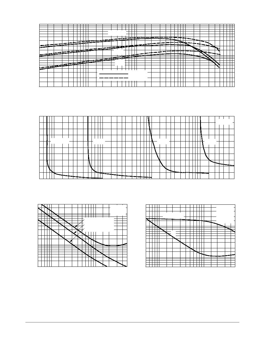
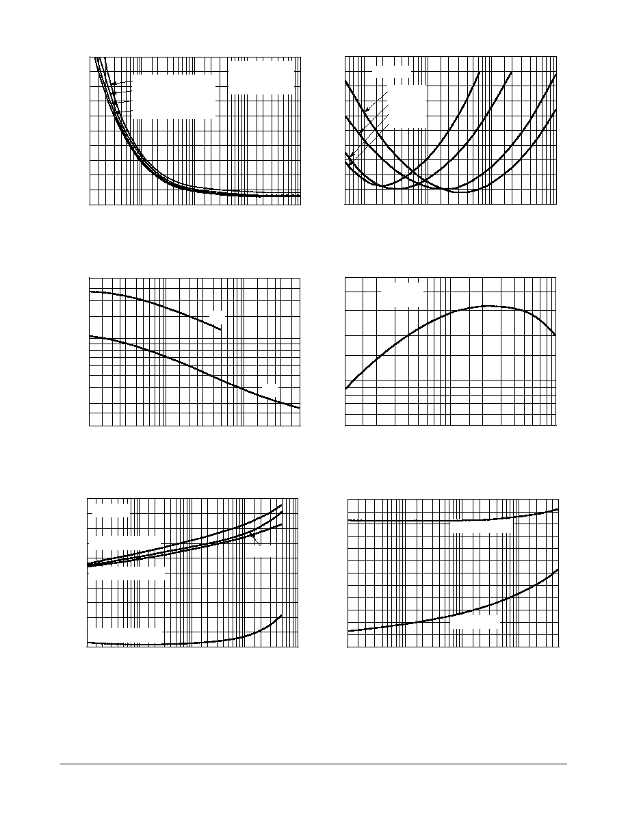
Figure 7. Frequency Effects
f, FREQUENCY (kHz)
4.0
6.0
8.0
10
2.0
0.1
Figure 8. Source Resistance Effects
R
S
, SOURCE RESISTANCE (OHMS)
NF
, NOISE FIGURE (dB)
1.0 2.0
5.0 10 20
50
0.2
0.5
0
100
NF
, NOISE FIGURE (dB)
0.01 0.02 0.05
R
S
= OPTIMUM
R
S
=
SOURCE
R
S
=
RESISTANCE
I
C
= 1.0 mA, R
S
= 150
500
µ
A, R
S
= 200
100
µ
A, R
S
= 2.0 k
50
µ
A, R
S
= 4.0 k
f = 1.0 kHz
I
C
= 50
µ
A
100
µ
A
500
µ
A
1.0 mA
4.0
6.0
8.0
10
2.0
0
50 100 200
500 1.0 k 2.0 k 5.0 k 10 k 20 k
50 k 100 k
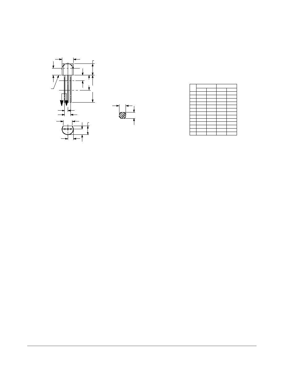
Figure 9. Capacitances
REVERSE VOLTAGE (VOLTS)
3.0
5.0
7.0
10
2.0
0.1
CAP
ACIT
ANCE (pF)
1.0
2.0 3.0 5.0 7.0 10
20 30
50
0.2 0.3 0.5 0.7
C
cb
20
30
C
eb
Figure 10. CurrentGain Bandwidth Product
I
C
, COLLECTOR CURRENT (mA)
70
100
200
300
50
500
f T
, CURRENT-GAIN BANDWIDTH PRODUCT
(MHz)
1.0
2.0 3.0
5.0 7.0 10
20 30
50 70 100
V
CE
= 20 V
T
J
= 25
°
C
Figure 11. "On" Voltages
I
C
, COLLECTOR CURRENT (mA)
0.4
0.6
0.8
1.0
0.2
V
,
VOL
T
AGE (VOL
TS)
0
T
J
= 25
°
C
V
BE(sat)
@ I
C
/I
B
= 10
V
CE(sat)
@ I
C
/I
B
= 10
V
BE(on)
@ V
CE
= 10 V
Figure 12. Temperature Coefficients
I
C
, COLLECTOR CURRENT (mA)
-0.5
0
+0.5
COEFFICIENT
(mV/ C)
-1.0
-1.5
-2.5
°
R
qVC
for V
CE(sat)
R
qVB
for V
BE
0.1
1.0 2.0
5.0 10 20
50
0.2
0.5
100 200 500 1.0 k
1.0 V
-2.0
0.1
1.0 2.0
5.0 10 20
50
0.2
0.5
100 200 500

PN2222, PN2222A
http://onsemi.com
8
ON Semiconductor and are trademarks of Semiconductor Components Industries, LLC (SCILLC). SCILLC reserves the right to make changes
without further notice to any products herein. SCILLC makes no warranty, representation or guarantee regarding the suitability of its products for any particular
purpose, nor does SCILLC assume any liability arising out of the application or use of any product or circuit, and specifically disclaims any and all liability,
including without limitation special, consequential or incidental damages. "Typical" parameters which may be provided in SCILLC data sheets and/or
specifications can and do vary in different applications and actual performance may vary over time. All operating parameters, including "Typicals" must be
validated for each customer application by customer's technical experts. SCILLC does not convey any license under its patent rights nor the rights of others.
SCILLC products are not designed, intended, or authorized for use as components in systems intended for surgical implant into the body, or other applications
intended to support or sustain life, or for any other application in which the failure of the SCILLC product could create a situation where personal injury or
death may occur. Should Buyer purchase or use SCILLC products for any such unintended or unauthorized application, Buyer shall indemnify and hold
SCILLC and its officers, employees, subsidiaries, affiliates, and distributors harmless against all claims, costs, damages, and expenses, and reasonable
attorney fees arising out of, directly or indirectly, any claim of personal injury or death associated with such unintended or unauthorized use, even if such claim
alleges that SCILLC was negligent regarding the design or manufacture of the part. SCILLC is an Equal Opportunity/Affirmative Action Employer.
PUBLICATION ORDERING INFORMATION
CENTRAL/SOUTH AMERICA:
Spanish Phone: 3033087143 (MonFri 8:00am to 5:00pm MST)
Email: ONlitspanish@hibbertco.com
TollFree from Mexico: Dial 018002882872 for Access
then Dial 8662979322
ASIA/PACIFIC: LDC for ON Semiconductor Asia Support
Phone: 3036752121 (TueFri 9:00am to 1:00pm, Hong Kong Time)
Toll Free from Hong Kong & Singapore:
00180044223781
Email: ONlitasia@hibbertco.com
JAPAN: ON Semiconductor, Japan Customer Focus Center
4321 NishiGotanda, Shinagawaku, Tokyo, Japan 1410031
Phone: 81357402700
Email: r14525@onsemi.com
ON Semiconductor Website: http://onsemi.com
For additional information, please contact your local
Sales Representative.
PN2222/D
NORTH AMERICA Literature Fulfillment:
Literature Distribution Center for ON Semiconductor
P.O. Box 5163, Denver, Colorado 80217 USA
Phone: 3036752175 or 8003443860 Toll Free USA/Canada
Fax: 3036752176 or 8003443867 Toll Free USA/Canada
Email: ONlit@hibbertco.com
Fax Response Line: 3036752167 or 8003443810 Toll Free USA/Canada
N. American Technical Support: 8002829855 Toll Free USA/Canada
EUROPE: LDC for ON Semiconductor European Support
German Phone: (+1) 3033087140 (MonFri 2:30pm to 7:00pm CET)
Email: ONlitgerman@hibbertco.com
French Phone: (+1) 3033087141 (MonFri 2:00pm to 7:00pm CET)
Email: ONlitfrench@hibbertco.com
English Phone: (+1) 3033087142 (MonFri 12:00pm to 5:00pm GMT)
Email: ONlit@hibbertco.com
EUROPEAN TOLLFREE ACCESS*: 0080044223781
*Available from Germany, France, Italy, UK, Ireland