
ę
Semiconductor Components Industries, LLC, 2000
November, 2000 ş Rev.3
1
Publication Order Number:
MTB60N06HD/D
MTB60N06HD
Preferred Device
Power MOSFET
60 Amps, 60 Volts
NşChannel D2PAK
This Power MOSFET is designed to withstand high energy in the
avalanche and commutation modes. The energy efficient design also
offers a drainştoşsource diode with a fast recovery time. Designed for
low voltage, high speed switching applications in power supplies,
converters and PWM motor controls, these devices are particularly
well suited for bridge circuits where diode speed and commutating
safe operating areas are critical and offer additional safety margin
against unexpected voltage transients.
Ě
Avalanche Energy Specified
Ě
SourceştoşDrain Diode Recovery Time Comparable to a
Discrete Fast Recovery Diode
Ě
Diode is Characterized for Use in Bridge Circuits
Ě
IDSS and VDS(on) Specified at Elevated Temperature
Ě
Short Heatsink Tab Manufactured ş Not Sheared
Ě
Specially Designed Leadframe for Maximum Power Dissipation
MAXIMUM RATINGS
(TC = 25
░
C unless otherwise noted)
Rating
Symbol
Value
Unit
DrainşSource Voltage
VDSS
60
Vdc
DrainşGate Voltage (RGS = 1.0 M
)
VDGR
60
Vdc
GateşSource Voltage
ş Continuous
ş NonşRepetitive (tp
10 ms)
VGS
VGSM
▒
20
▒
30
Vdc
Vpk
Drain Current ş Continuous
Drain Current
ş Continuous @ 100
░
C
Drain Current
ş Single Pulse (tp
10
Á
s)
ID
ID
IDM
60
42.3
180
Adc
Apk
Total Power Dissipation
Derate above 25
░
C
Total Power Dissipation @ TA = 25
░
C
(Note 1.)
PD
125
1.0
2.5
Watts
W/
░
C
Watts
Operating and Storage Temperature
Range
TJ, Tstg
ş 55 to
150
░
C
Single Pulse DrainştoşSource Avalanche
Energy ş Starting TJ = 25
░
C
(VDD = 25 Vdc, VGS = 10 Vdc, Peak
IL = 60 Apk, L = 0.3 mH, RG = 25
)
EAS
540
mJ
Thermal Resistance
ş Junction to Case
ş Junction to Ambient
ş Junction to Ambient, when mounted
with the minimum recommended pad size
R
JC
R
JA
R
JA
1.0
62.5
50
░
C/W
Maximum Lead Temperature for Soldering
Purposes, 1/8
from case for 10
seconds
TL
260
░
C
1. When mounted with the minimum recommended pad size.
MARKING DIAGRAM
& PIN ASSIGNMENT
T60N06HD
YWW
1
Gate
4
Drain
2
Drain
3
Source
60 AMPERES
60 VOLTS
RDS(on) = 14 m
Device
Package
Shipping
ORDERING INFORMATION
MTB60N06HD
D2PAK
50 Units/Rail
D2PAK
CASE 418B
STYLE 2
1
2
3
4
http://onsemi.com
NşChannel
D
S
G
T60N06HD
= Device Code
Y
= Year
WW
= Work Week
MTB60N06HDT4
D2PAK
800/Tape & Reel
Preferred devices are recommended choices for future use
and best overall value.

MTB60N06HD
http://onsemi.com
2
ELECTRICAL CHARACTERISTICS
(TJ = 25
░
C unless otherwise noted)
Characteristic
Symbol
Min
Typ
Max
Unit
OFF CHARACTERISTICS
DrainştoşSource Breakdown Voltage
(Cpk
2.0) (Note 4.)
(VGS = 0 Vdc, ID = 250
Á
Adc)
Temperature Coefficient (Positive)
V(BR)DSS
60
ş
ş
71
ş
ş
Vdc
mV/
░
C
Zero Gate Voltage Drain Current
(VDS = 60 Vdc, VGS = 0 Vdc)
(VDS = 60 Vdc, VGS = 0 Vdc, TJ = 125
░
C)
IDSS
ş
ş
ş
ş
10
100
Á
Adc
GateşBody Leakage Current
(VGS =
▒
20 Vdc, VDS = 0 Vdc)
IGSS
ş
ş
100
nAdc
ON CHARACTERISTICS (Note 2.)
Gate Threshold Voltage
(Cpk
3.0) (Note 4.)
(VDS = VGS, ID = 250
Á
Adc)
Threshold Temperature Coefficient (Negative)
VGS(th)
2.0
ş
3.0
7.0
4.0
ş
Vdc
mV/
░
C
Static DrainşSource OnşResistance
(Cpk
3.0) (Note 4.)
(VGS = 10 Vdc, ID = 30 Adc)
RDS(on)
ş
0.011
0.014
Ohm
DrainşSource OnşVoltage (VGS = 10 Vdc)
(ID = 60 Adc)
(ID = 30 Adc, TJ =125
░
C)
VDS(on)
ş
ş
ş
ş
1.0
0.9
Vdc
Forward Transconductance
(VDS = 4.0 Vdc, ID = 30 Adc)
gFS
15
20
ş
mhos
DYNAMIC CHARACTERISTICS
Input Capacitance
(V
25 Vd
V
0 Vd
Ciss
ş
1950
2800
pF
Output Capacitance
(VDS = 25 Vdc, VGS = 0 Vdc,
f = 1.0 MHz)
Coss
ş
660
920
Transfer Capacitance
f = 1.0 MHz)
Crss
ş
147
300
SWITCHING CHARACTERISTICS (Note 3.)
TurnşOn Delay Time
td(on)
ş
14
26
ns
Rise Time
(VDD= 30 Vdc, ID = 60 Adc,
VGS = 10 Vdc
tr
ş
197
394
TurnşOff Delay Time
VGS = 10 Vdc,
RG = 9.1
)
td(off)
ş
50
102
Fall Time
RG 9.1
)
tf
ş
124
246
Gate Charge
(S
Fi
8)
QT
ş
51
71
nC
(See Figure 8)
(VDS = 48 Vdc, ID = 60 Adc,
Q1
ş
12
ş
(VDS 48 Vdc, ID 60 Adc,
VGS = 10 Vdc)
Q2
ş
24
ş
Q3
ş
21
ş
SOURCEşDRAIN DIODE CHARACTERISTICS
Forward OnşVoltage
(IS = 60 Adc, VGS = 0 Vdc)
(IS = 60 Adc, VGS = 0 Vdc,
TJ = 125
░
C)
VSD
ş
ş
0.99
0.89
1.0
ş
Vdc
Reverse Recovery Time
(S
Fi
15)
trr
ş
60
ş
ns
(See Figure 15)
(IS = 60 Adc, VGS = 0 Vdc,
ta
ş
36
ş
(IS 60 Adc, VGS 0 Vdc,
dIS/dt = 100 A/
Á
s)
tb
ş
24
ş
Reverse Recovery Stored Charge
QRR
ş
0.143
ş
Á
C
INTERNAL PACKAGE INDUCTANCE
Internal Drain Inductance
(Measured from the drain lead 0.25
from package to center of die)
LD
ş
4.5
ş
nH
Internal Source Inductance
(Measured from the source lead 0.25
from package to source bond pad)
LS
ş
7.5
ş
nH
2. Pulse Test: Pulse Width
300
Á
s, Duty Cycle
2%.
3. Switching characteristics are independent of operating junction temperature.
4. Reflects typical values.
Cpk =
Max limit ş Typ
3 x SIGMA

MTB60N06HD
http://onsemi.com
3
TYPICAL ELECTRICAL CHARACTERISTICS
R DS(on)
, DRAIN-T
O-SOURCE RESIST
ANCE
(NORMALIZED)
R DS(on)
, DRAIN-T
O-SOURCE RESIST
ANCE (OHMS)
R DS(on)
, DRAIN-T
O-SOURCE RESIST
ANCE (OHMS)
ID, DRAIN CURRENT (AMPS)
TJ, JUNCTION TEMPERATURE (
░
C)
VDS, DRAIN-TO-SOURCE VOLTAGE (VOLTS)
I DSS
, LEAKAGE (nA)
ID, DRAIN CURRENT (AMPS)
I D
, DRAIN CURRENT
(AMPS)
VDS, DRAIN-TO-SOURCE VOLTAGE (VOLTS)
VGS, GATE-TO-SOURCE VOLTAGE (VOLTS)
I D
, DRAIN CURRENT
(AMPS)
0
20
40
80
120
100
60
0
1.0
2.0
3.0
4.0
5.0
0
20
40
80
120
Figure 1. OnşRegion Characteristics
2.0
2.8
3.6
4.4
6.0
7.6
Figure 2. Transfer Characteristics
0
20
40
60
80
120
0.006
0.008
0.012
0.016
0.020
0.0100
0.0108
0.0116
0.0124
0.0132
Figure 3. OnşResistance versus Drain Current
and Temperature
Figure 4. OnşResistance versus Drain Current
and Gate Voltage
- 50
0.6
0.8
1.0
1.4
1.8
0
10
20
40
50
60
1
10
100
1000
Figure 5. OnşResistance Variation with
Temperature
Figure 6. DrainştoşSource Leakage
Current versus Voltage
- 25
0
25
50
75
100
125
150
100
60
0.5
1.5
2.5
3.5
4.5
6.8
0.018
0.014
0.010
100
0
20
40
60
80
120
100
0.0128
0.0120
0.0112
0.0104
1.2
1.6
30
VGS = 10 V
9 V
8 V
100
░
C
25
░
C
TJ = - 55
░
C
TJ = 25
░
C
15 V
VGS = 10 V
VGS = 10 V
- 55
░
C
VGS = 0 V
TJ = 125
░
C
100
░
C
25
░
C
5 V
6 V
TJ = 25
░
C
7 V
10
30
50
70
90
110
10
30
50
70
90
110
VDS
10 V
5.2
VGS = 10 V
ID = 30 A
TJ = 100
░
C
25
░
C

MTB60N06HD
http://onsemi.com
4
POWER MOSFET SWITCHING
Switching behavior is most easily modeled and predicted
by recognizing that the power MOSFET is charge
controlled. The lengths of various switching intervals (
t)
are determined by how fast the FET input capacitance can
be charged by current from the generator.
The published capacitance data is difficult to use for
calculating rise and fall because drainşgate capacitance
varies greatly with applied voltage. Accordingly, gate
charge data is used. In most cases, a satisfactory estimate of
average input current (IG(AV)) can be made from a
rudimentary analysis of the drive circuit so that
t = Q/IG(AV)
During the rise and fall time interval when switching a
resistive load, VGS remains virtually constant at a level
known as the plateau voltage, VSGP. Therefore, rise and fall
times may be approximated by the following:
tr = Q2 x RG/(VGG ş VGSP)
tf = Q2 x RG/VGSP
where
VGG = the gate drive voltage, which varies from zero to VGG
RG = the gate drive resistance
and Q2 and VGSP are read from the gate charge curve.
During the turnşon and turnşoff delay times, gate current is
not constant. The simplest calculation uses appropriate
values from the capacitance curves in a standard equation for
voltage change in an RC network. The equations are:
td(on) = RG Ciss In [VGG/(VGG ş VGSP)]
td(off) = RG Ciss In (VGG/VGSP)
The capacitance (Ciss) is read from the capacitance curve at
a voltage corresponding to the offşstate condition when
calculating td(on) and is read at a voltage corresponding to the
onşstate when calculating td(off).
At high switching speeds, parasitic circuit elements
complicate the analysis. The inductance of the MOSFET
source lead, inside the package and in the circuit wiring
which is common to both the drain and gate current paths,
produces a voltage at the source which reduces the gate drive
current. The voltage is determined by Ldi/dt, but since di/dt
is a function of drain current, the mathematical solution is
complex. The MOSFET output capacitance also
complicates the mathematics. And finally, MOSFETs have
finite internal gate resistance which effectively adds to the
resistance of the driving source, but the internal resistance
is difficult to measure and, consequently, is not specified.
The resistive switching time variation versus gate
resistance (Figure 9) shows how typical switching
performance is affected by the parasitic circuit elements. If
the parasitics were not present, the slope of the curves would
maintain a value of unity regardless of the switching speed.
The circuit used to obtain the data is constructed to minimize
common inductance in the drain and gate circuit loops and
is believed readily achievable with board mounted
components. Most power electronic loads are inductive; the
data in the figure is taken with a resistive load, which
approximates an optimally snubbed inductive load. Power
MOSFETs may be safely operated into an inductive load;
however, snubbing reduces switching losses.
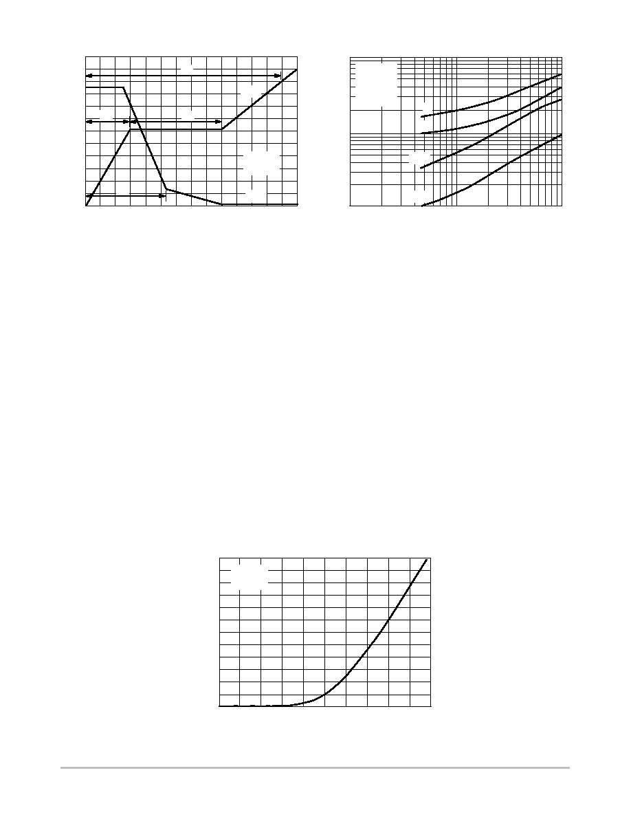
GATE-TO-SOURCE OR DRAIN-TO-SOURCE VOLTAGE (VOLTS)
C, CAP
ACIT
ANCE (pF)
0
1000
2000
3000
5000
Figure 7. Capacitance Variation
4000
10
0
10
15
20
25
VGS
VDS
5
5
VDS = 0 V
Ciss
Crss
VGS = 0 V
TJ = 25
░
C
Ciss
Coss
Crss
MTB60N06HD
http://onsemi.com
5
QT, TOTAL GATE CHARGE (nC)
RG, GATE RESISTANCE (Ohms)
t, TIME
(ns)
V DS
, DRAIN-T
O-SOURCE VOL
T
AGE (VOL
TS)
V GS
, GA
TE-T
O-SOURCE VOL
T
AGE (VOL
TS)
Figure 8. GateşToşSource and DrainşToşSource
Voltage versus Total Charge
1
10
100
10
100
1000
VDD = 30 V
ID = 60 A
VGS = 10 V
TJ = 25
░
C
tr
tf
td(on)
td(off)
Figure 9. Resistive Switching Time
Variation versus Gate Resistance
0
8
24
40
48
56
16
32
10
6
2
0
8
4
12
60
50
40
30
10
20
0
QT
Q2
VGS
ID = 60 A
TJ = 25
░
C
VDS
Q3
Q1
DRAINşTOşSOURCE DIODE CHARACTERISTICS
The switching characteristics of a MOSFET body diode
are very important in systems using it as a freewheeling or
commutating diode. Of particular interest are the reverse
recovery characteristics which play a major role in
determining switching losses, radiated noise, EMI and RFI.
System switching losses are largely due to the nature of
the body diode itself. The body diode is a minority carrier
device, therefore it has a finite reverse recovery time, trr, due
to the storage of minority carrier charge, QRR, as shown in
the typical reverse recovery wave form of Figure 12. It is this
stored charge that, when cleared from the diode, passes
through a potential and defines an energy loss. Obviously,
repeatedly forcing the diode through reverse recovery
further increases switching losses. Therefore, one would
like a diode with short trr and low QRR specifications to
minimize these losses.
The abruptness of diode reverse recovery effects the
amount of radiated noise, voltage spikes, and current
ringing. The mechanisms at work are finite irremovable
circuit parasitic inductances and capacitances acted upon by
high di/dts. The diode's negative di/dt during ta is directly
controlled by the device clearing the stored charge.
However, the positive di/dt during tb is an uncontrollable
diode characteristic and is usually the culprit that induces
current ringing. Therefore, when comparing diodes, the
ratio of tb/ta serves as a good indicator of recovery
abruptness and thus gives a comparative estimate of
probable noise generated. A ratio of 1 is considered ideal and
values less than 0.5 are considered snappy.
Compared to ON Semiconductor standard cell density
low voltage MOSFETs, high cell density MOSFET diodes
are faster (shorter trr), have less stored charge and a softer
reverse recovery characteristic. The softness advantage of
the high cell density diode means they can be forced through
reverse recovery at a higher di/dt than a standard cell
MOSFET diode without increasing the current ringing or the
noise generated. In addition, power dissipation incurred
from switching the diode will be less due to the shorter
recovery time and lower switching losses.
I S
, SOURCE CURRENT
(AMPS)
VSD, SOURCE-TO-DRAIN VOLTAGE (VOLTS)
Figure 10. Diode Forward Voltage versus Current
0
10
30
50
60
40
20
0.5
0.6
0.7
0.8
0.9
1.0
VGS = 0 V
TJ = 25
░
C