
©
Semiconductor Components Industries, LLC, 2001
October, 2001 - Rev. 1
1
Publication Order Number:
MPSA05/D
MPSA05, MPSA06, MPSA55,
MPSA56
MPSA06 and MPSA56 are Preferred Devices
Amplifier Transistors
Voltage and Current are Negative
for PNP Transistors
COLLECTOR
3
2
BASE
1
EMITTER
STYLE 1
MPSA05, MPSA06
NPN
COLLECTOR
3
2
BASE
1
EMITTER
STYLE 1
MPSA55, MPSA56
PNP
MAXIMUM RATINGS
Rating
Symbol
Value
Unit
Collector - Emitter Voltage
MPSA05, MPSA55
MPSA06, MPSA56
V
CEO
60
80
Vdc
Collector - Base Voltage
MPSA05, MPSA55
MPSA06, MPSA56
V
CBO
60
80
Vdc
Emitter - Base Voltage
V
EBO
4.0
Vdc
Collector Current - Continuous
I
C
500
mAdc
Total Device Dissipation
@ T
A
= 25
°
C
Derate above 25
°
C
P
D
625
5.0
mW
mW/
°
C
Total Device Dissipation
@ T
C
= 25
°
C
Derate above 25
°
C
P
D
1.5
12
Watts
mW/
°
C
Operating and Storage Junction
Temperature Range
T
J
, T
stg
- 55 to
+150
°
C
THERMAL CHARACTERISTICS
Characteristic
Symbol
Max
Unit
Thermal Resistance,
Junction to Ambient
R
JA
(Note 1.)
200
°
C/W
Thermal Resistance,
Junction to Case
R
JC
83.3
°
C/W
1. R
q
JA
is measured with the device soldered into a typical printed circuit board.
Device
Package
Shipping
ORDERING INFORMATION
MPSA05
TO-92
http://onsemi.com
TO-92
CASE 29
STYLE 1
5000 Units/Box
3
2
1
Preferred devices are recommended choices for future use
and best overall value.
MPSA05RLRA
TO-92
2000/Tape & Reel
MPSA05RLRM
TO-92
2000/Ammo Pack
MPSA06
TO-92
5000 Units/Box
MPSA06RLRA
TO-92
2000/Tape & Reel
MPSA06RLRM
TO-92
2000/Ammo Pack
MARKING DIAGRAM
MPS
Axxx
YWW
MPSA06RLRP
TO-92
2000/Ammo Pack
NPN
MPSA05, MPSA06
PNP
MPSA55, MPSA56
MPSA55
TO-92
5000 Units/Box
MPSA55RLRA
TO-92
2000/Tape & Reel
MPSA56
TO-92
5000 Units/Box
MPSA56RLRA
TO-92
2000/Tape & Reel
MPSA56RLRM
TO-92
2000/Ammo Pack
MPSA56RLRP
TO-92
2000/Ammo Pack
MPSA
= Specific Device Code
xxx
= 05, 06, 55 or 56
Y
= Year
WW
= Work Week
MPSA05, MPSA06, MPSA55, MPSA56
http://onsemi.com
2
ELECTRICAL CHARACTERISTICS
(T
A
= 25
°
C unless otherwise noted)
Characteristic
Symbol
Min
Max
Unit
OFF CHARACTERISTICS
Collector - Emitter Breakdown Voltage (Note 2.)
(I
C
= 1.0 mAdc, I
B
= 0)
MPSA05, MPSA55
MPSA06, MPSA56
V
(BR)CEO
60
80
-
-
Vdc
Emitter - Base Breakdown Voltage (I
E
= 100
µ
Adc, I
C
= 0)
V
(BR)EBO
4.0
-
Vdc
Collector Cutoff Current (V
CE
= 60 Vdc, I
B
= 0)
I
CES
-
0.1
µ
Adc
Collector Cutoff Current
(V
CB
= 60 Vdc, I
E
= 0)
MPSA05, MPSA55
(V
CB
= 80 Vdc, I
E
= 0)
MPSA06, MPSA56
I
CBO
-
-
0.1
0.1
µ
Adc
ON CHARACTERISTICS
DC Current Gain
(I
C
= 10 mAdc, V
CE
= 1.0 Vdc)
(I
C
= 100 mAdc, V
CE
= 1.0 Vdc)
h
FE
100
100
-
-
-
Collector - Emitter Saturation Voltage
(I
C
= 100 mAdc, I
B
= 10 mAdc)
V
CE(sat)
-
0.25
Vdc
Base-Emitter On Voltage
(I
C
= 100 mAdc, V
CE
= 1.0 Vdc)
V
BE(on)
-
1.2
Vdc
SMALL-SIGNAL CHARACTERISTICS
Current - Gain - Bandwidth Product (Note 3.)
(I
C
= 10 mA, V
CE
= 2.0 V, f = 100 MHz)
MPSA05
MPSA06
(I
C
= 100 mAdc, V
CE
= 1.0 Vdc, f = 100 MHz)
MPSA55
MPSA56
f
T
100
50
-
-
MHz
2. Pulse Test: Pulse Width
v
300
m
s, Duty Cycle
v
2%.
3. f
T
is defined as the frequency at which |h
fe
| extrapolates to unity.
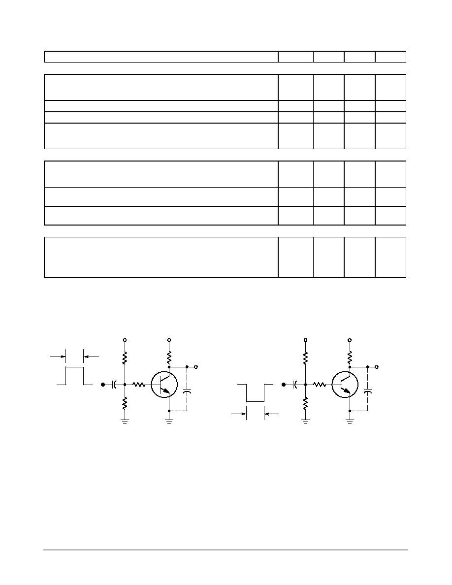
Figure 1. Switching Time Test Circuits
OUTPUT
TURN-ON TIME
-1.0 V
V
CC
+40 V
R
L
* C
S
t 6.0 pF
R
B
100
100
V
in
5.0 mF
t
r
= 3.0 ns
0
+10 V
5.0 ms
OUTPUT
TURN-OFF TIME
+V
BB
V
CC
+40 V
R
L
* C
S
t 6.0 pF
R
B
100
100
V
in
5.0 mF
t
r
= 3.0 ns
5.0 ms
*Total Shunt Capacitance of Test Jig and Connectors
For PNP Test Circuits, Reverse All Voltage Polarities

MPSA05, MPSA06, MPSA55, MPSA56
http://onsemi.com
3
Figure 2. MPSA05/06 Current-Gain --
Bandwidth Product
Figure 3. MPSA55/56 Current-Gain --
Bandwidth Product
Figure 4. MPSA05/06 Capacitance
Figure 5. MPSA55/56 Capacitance
Figure 6. MPSA05/06 Switching Time
Figure 7. MPSA55/56 Switching Time
100
200
2.0
I
C
, COLLECTOR CURRENT (mA)
300
200
100
70
50
30
I
C
, COLLECTOR CURRENT (mA)
-100
-200
-10
200
100
70
50
20
10
100
0.1
V
R
, REVERSE VOLTAGE (VOLTS)
80
60
40
20
10
8.0
V
R
, REVERSE VOLTAGE (VOLTS)
-1.0
-100
-0.1
100
70
50
30
20
10
-2.0
20
V
CE
= 2.0 V
T
J
= 25
°
C
V
CE
= -2.0 V
T
J
= 25
°
C
T
J
= 25
°
C
f T
, CURRENT-GAIN - BANDWIDTH PRODUCT
(MHz)
NPN
PNP
C, CAP
ACIT
ANCE (pF)
3.0
5.0 7.0 10
20
30
50 70
-2.0 -3.0
-5.0 -7.0
-20 -30
-50 -70
30
f T
, CURRENT-GAIN - BANDWIDTH PRODUCT
(MHz)
50
1.0
2.0
5.0
0.2
0.5
6.0
4.0
C
ibo
C
obo
7.0
5.0
-0.2
-0.5
-5.0
-10 -20
-50
T
J
= 25
°
C
C
ibo
C
obo
20
10
I
C
, COLLECTOR CURRENT (mA)
200
100
50
20
10
I
C
, COLLECTOR CURRENT (mA)
-10
-5.0
500
200
100
50
20
10
-100
100
t, TIME
(ns)
t, TIME
(ns)
50
200
500
1.0 k
500
V
CC
= 40 V
I
C
/I
B
= 10
I
B1
= I
B2
T
J
= 25
°
C
t
s
t
f
t
r
-50
-200
-500
1.0 k
5.0 7.0
30
70
300
700
30
70
t
d
@ V
BE(off)
= 0.5 V
300
700
70
30
-7.0
-300
-70
-20 -30
V
CC
= -40 V
I
C
/I
B
= 10
I
B1
= I
B2
T
J
= 25
°
C
t
s
t
f
t
r
t
d
@ V
BE(off)
= -0.5 V
C, CAP
ACIT
ANCE (pF)
300

MPSA05, MPSA06, MPSA55, MPSA56
http://onsemi.com
4
Figure 8. MPSA05/06 Active-Region Safe
Operating Area
Figure 9. MPSA55/56 Active-Region Safe
Operating Area
Figure 10. MPSA05/06 DC Current Gain
Figure 11. MPSA55/56 DC Current Gain
Figure 12. MPSA05/06 "ON" Voltages
Figure 13. MPSA55/56 "ON" Voltages
2.0
500
0.5
I
C
, COLLECTOR CURRENT (mA)
400
200
100
80
60
40
10
, DC CURRENT
GAIN
NPN
PNP
T
J
= 125
°
C
10
500
1.0
I
C
, COLLECTOR CURRENT (mA)
1.0
0.8
0.6
0.4
0.2
0
100
T
J
= 25
°
C
V
,
VOL
T
AGE (VOL
TS)
V
,
VOL
T
AGE (VOL
TS)
V
BE(sat)
@ I
C
/I
B
= 10
V
CE(sat)
@ I
C
/I
B
= 10
V
BE(on)
@ V
CE
= 1.0 V
10
1.0
V
CE
, COLLECTOR-EMITTER VOLTAGE (VOLTS)
500
200
100
50
20
10
V
CE
, COLLECTOR-EMITTER VOLTAGE (VOLTS)
-10
-50
-1.0
-500
-200
-100
-50
-20
-10
-20
30
I C
, COLLECT
OR CURRENT
(mA)
-2.0
-5.0
-1.0 k
2.0
5.0
50
1.0 k
I C
, COLLECT
OR CURRENT
(mA)
1.0 ms
1.0 s
T
A
= 25
°
C
MPSA05
CURRENT LIMIT
THERMAL LIMIT
SECOND BREAKDOWN LIMIT
MPSA06
100
70
20
3.0
7.0
100 ms
T
C
= 25
°
C
1.0
3.0 5.0
V
CE
= 1.0 V
20
100
30 50
200 300
h
FE
25
°
C
-55
°
C
0.5
2.0
5.0
200
20
50
-2.0
-500
-0.5
I
C
, COLLECTOR CURRENT (mA)
400
200
100
80
60
40
-10
, DC CURRENT
GAIN
T
J
= 125
°
C
-1.0
-5.0
V
CE
= -1.0 V
-20
-100
-50
-200
h
FE
25
°
C
-55
°
C
-10
-500
-1.0
I
C
, COLLECTOR CURRENT (mA)
-1.0
-0.8
-0.6
-0.4
-0.2
0
-100
T
J
= 25
°
C
V
BE(sat)
@ I
C
/I
B
= 10
V
CE(sat)
@ I
C
/I
B
= 10
V
BE(on)
@ V
CE
= -1.0 V
-0.5
-2.0
-5.0
-200
-20
-50
700
300
30
70
1.0 ms
1.0 s
T
A
= 25
°
C
MPSA55
CURRENT LIMIT
THERMAL LIMIT
SECOND BREAKDOWN LIMIT
MPSA56
100 ms
T
C
= 25
°
C
-3.0
-7.0
-30
-100
-70
-30
-70
-300
-700

MPSA05, MPSA06, MPSA55, MPSA56
http://onsemi.com
5
Figure 14. MPSA05/06 Collector Saturation
Region
Figure 15. MPSA55/56 Collector Saturation
Region
Figure 16. MPSA05/06 Base-Emitter
Temperature Coefficient
Figure 17. MPSA55/56 Base-Emitter
Temperature Coefficient
100
500
0.5
I
C
, COLLECTOR CURRENT (mA)
-0.8
-1.2
-1.6
-2.0
-2.4
-2.8
I
C
, COLLECTOR CURRENT (mA)
0.1
10
0.05
I
B
, BASE CURRENT (mA)
1.0
0.8
0.6
0.4
0.2
0
I
B
, BASE CURRENT (mA)
1.0
T
J
= 25
°
C
R
VB
,
TEMPERA
TURE COEFFICIENT
(mV/ C)
NPN
PNP
10
R
qVB
for V
BE
q
°
R
VB
,
TEMPERA
TURE COEFFICIENT
(mV/ C)
q
°
50
I
C
=
100 mA
I
C
=
50 mA
I
C
=
250 mA
I
C
=
500 mA
I
C
=
10 mA
, COLLECT
OR-EMITTER VOL
T
AGE (VOL
TS)
V
CE
, COLLECT
OR-EMITTER VOL
T
AGE (VOL
TS)
V
CE
1.0
2.0
5.0
20
50
200
20
2.0
5.0
0.2
0.5
-100
-500
-0.5
-0.8
-1.2
-1.6
-2.0
-2.4
-2.8
-10
R
qVB
for V
BE
-1.0 -2.0
-5.0
-20
-50
-200
-0.1
-10
-0.05
-1.0
-0.8
-0.6
-0.4
-0.2
0
-1.0
T
J
= 25
°
C
-50
I
C
=
-100 mA
I
C
=
-50 mA
I
C
=
-250 mA
I
C
=
-500 mA
I
C
=
-10 mA
-20
-2.0
-5.0
-0.2
-0.5
Figure 18. MPSA05, MPSA06, MPSA55 and MPSA56 Thermal Response
t, TIME (ms)
1.0
2.0
5.0
10
20
50
100
200
500
1.0 k
2.0 k
5.0 k
10 k
20 k
50 k 100 k
0.03
0.02
0.1
0.07
0.05
0.01
0.3
0.2
1.0
0.7
0.5
r(t), NORMALIZED
TRANSIENT
THERMAL
RESIST
ANCE
Z
JC
(t) = r(t)
·
R
JC
T
J(pk)
- T
C
= P
(pk)
Z
JC
(t)
Z
JA
(t) = r(t)
·
R
JA
T
J(pk)
- T
A
= P
(pk)
Z
JA
(t)
D CURVES APPLY FOR
POWER PULSE TRAIN
SHOWN READ TIME AT t
1
(SEE AN469)
t
1
t
2
DUTY CYCLE, D = t
1
/t
2
P
(pk)
D = 0.5
0.2
0.1
0.02
0.01
SINGLE PULSE
SINGLE PULSE
0.05

MPSA05, MPSA06, MPSA55, MPSA56
http://onsemi.com
6
PACKAGE DIMENSIONS
TO-92
TO-226AA
CASE 29-11
ISSUE AL
NOTES:
1. DIMENSIONING AND TOLERANCING PER ANSI
Y14.5M, 1982.
2. CONTROLLING DIMENSION: INCH.
3. CONTOUR OF PACKAGE BEYOND DIMENSION R
IS UNCONTROLLED.
4. LEAD DIMENSION IS UNCONTROLLED IN P AND
BEYOND DIMENSION K MINIMUM.
R
A
P
J
L
B
K
G
H
SECTION X-X
C
V
D
N
N
X X
SEATING
PLANE
DIM
MIN
MAX
MIN
MAX
MILLIMETERS
INCHES
A
0.175
0.205
4.45
5.20
B
0.170
0.210
4.32
5.33
C
0.125
0.165
3.18
4.19
D
0.016
0.021
0.407
0.533
G
0.045
0.055
1.15
1.39
H
0.095
0.105
2.42
2.66
J
0.015
0.020
0.39
0.50
K
0.500
---
12.70
---
L
0.250
---
6.35
---
N
0.080
0.105
2.04
2.66
P
---
0.100
---
2.54
R
0.115
---
2.93
---
V
0.135
---
3.43
---
1
STYLE 1:
PIN 1. EMITTER
2. BASE
3. COLLECTOR
STYLE 14:
PIN 1. EMITTER
2. COLLECTOR
3. BASE

MPSA05, MPSA06, MPSA55, MPSA56
http://onsemi.com
7
Notes

MPSA05, MPSA06, MPSA55, MPSA56
http://onsemi.com
8
ON Semiconductor and are trademarks of Semiconductor Components Industries, LLC (SCILLC). SCILLC reserves the right to make changes
without further notice to any products herein. SCILLC makes no warranty, representation or guarantee regarding the suitability of its products for any particular
purpose, nor does SCILLC assume any liability arising out of the application or use of any product or circuit, and specifically disclaims any and all liability,
including without limitation special, consequential or incidental damages. "Typical" parameters which may be provided in SCILLC data sheets and/or
specifications can and do vary in different applications and actual performance may vary over time. All operating parameters, including "Typicals" must be
validated for each customer application by customer's technical experts. SCILLC does not convey any license under its patent rights nor the rights of others.
SCILLC products are not designed, intended, or authorized for use as components in systems intended for surgical implant into the body, or other applications
intended to support or sustain life, or for any other application in which the failure of the SCILLC product could create a situation where personal injury or
death may occur. Should Buyer purchase or use SCILLC products for any such unintended or unauthorized application, Buyer shall indemnify and hold
SCILLC and its officers, employees, subsidiaries, affiliates, and distributors harmless against all claims, costs, damages, and expenses, and reasonable
attorney fees arising out of, directly or indirectly, any claim of personal injury or death associated with such unintended or unauthorized use, even if such claim
alleges that SCILLC was negligent regarding the design or manufacture of the part. SCILLC is an Equal Opportunity/Affirmative Action Employer.
PUBLICATION ORDERING INFORMATION
JAPAN: ON Semiconductor, Japan Customer Focus Center
4-32-1 Nishi-Gotanda, Shinagawa-ku, Tokyo, Japan 141-0031
Phone: 81-3-5740-2700
Email: r14525@onsemi.com
ON Semiconductor Website: http://onsemi.com
For additional information, please contact your local
Sales Representative.
MPSA05/D
Literature Fulfillment:
Literature Distribution Center for ON Semiconductor
P.O. Box 5163, Denver, Colorado 80217 USA
Phone: 303-675-2175 or 800-344-3860 Toll Free USA/Canada
Fax: 303-675-2176 or 800-344-3867 Toll Free USA/Canada
Email: ONlit@hibbertco.com
N. American Technical Support: 800-282-9855 Toll Free USA/Canada