®
Semiconductor Components Industries, LLC, 2004
April, 2004 - Rev. 4
1
Publication Order Number:
2N3055/D
2N3055, MJ2955
Preferred Device
Complementary Silicon
Power Transistors
. . . designed for general-purpose switching and amplifier
applications.
À
DC Current Gain - h
FE
= 20 -70 @ I
C
= 4 Adc
À
Collector-Emitter Saturation Voltage -
V
CE(sat)
= 1.1 Vdc (Max) @ I
C
= 4 Adc
À
Excellent Safe Operating Area
À
Pb-Free Package is Available
MAXIMUM RATINGS
╬╬╬╬╬╬╬╬╬╬╬╬
╬╬╬╬╬╬╬╬╬╬╬╬
Rating
╬╬╬
╬╬╬
Symbol
╬╬╬╬╬
╬╬╬╬╬
Value
╬╬
╬╬
Unit
╬╬╬╬╬╬╬╬╬╬╬╬
╬╬╬╬╬╬╬╬╬╬╬╬
Collector-Emitter Voltage
╬╬╬
╬╬╬
V
CEO
╬╬╬╬╬
╬╬╬╬╬
60
╬╬
╬╬
Vdc
╬╬╬╬╬╬╬╬╬╬╬╬
╬╬╬╬╬╬╬╬╬╬╬╬
Collector-Emitter Voltage
╬╬╬
╬╬╬
V
CER
╬╬╬╬╬
╬╬╬╬╬
70
╬╬
╬╬
Vdc
╬╬╬╬╬╬╬╬╬╬╬╬
╬
╬╬╬╬╬╬╬╬╬╬
╬
╬╬╬╬╬╬╬╬╬╬╬╬
Collector-Base Voltage
╬╬╬
╬
╬
╬
╬╬╬
V
CB
╬╬╬╬╬
╬
╬╬╬
╬
╬╬╬╬╬
100
╬╬
╬╬
╬╬
Vdc
╬╬╬╬╬╬╬╬╬╬╬╬
╬╬╬╬╬╬╬╬╬╬╬╬
Emitter-Base Voltage
╬╬╬
╬╬╬
V
EB
╬╬╬╬╬
╬╬╬╬╬
7
╬╬
╬╬
Vdc
╬╬╬╬╬╬╬╬╬╬╬╬
╬╬╬╬╬╬╬╬╬╬╬╬
Collector Current - Continuous
╬╬╬
╬╬╬
I
C
╬╬╬╬╬
╬╬╬╬╬
15
╬╬
╬╬
Adc
╬╬╬╬╬╬╬╬╬╬╬╬
╬╬╬╬╬╬╬╬╬╬╬╬
Base Current
╬╬╬
╬╬╬
I
B
╬╬╬╬╬
╬╬╬╬╬
7
╬╬
╬╬
Adc
╬╬╬╬╬╬╬╬╬╬╬╬
╬
╬╬╬╬╬╬╬╬╬╬
╬
╬╬╬╬╬╬╬╬╬╬╬╬
Total Power Dissipation @ T
C
= 25
░
C
Derate above 25
░
C
╬╬╬
╬
╬
╬
╬╬╬
P
D
╬╬╬╬╬
╬
╬╬╬
╬
╬╬╬╬╬
115
0.657
╬╬
╬╬
╬╬
W
W/
░
C
╬╬╬╬╬╬╬╬╬╬╬╬
╬
╬╬╬╬╬╬╬╬╬╬
╬
╬╬╬╬╬╬╬╬╬╬╬╬
Operating and Storage Junction Tempera-
ture Range
╬╬╬
╬
╬
╬
╬╬╬
T
J
, T
stg
╬╬╬╬╬
╬
╬╬╬
╬
╬╬╬╬╬
¡ 65 to + 200
╬╬
╬╬
╬╬
░
C
THERMAL CHARACTERISTICS
╬╬╬╬╬╬╬╬╬╬╬╬
╬╬╬╬╬╬╬╬╬╬╬╬
Characteristic
╬╬╬
╬╬╬
Symbol
╬╬╬╬╬
╬╬╬╬╬
Max
╬╬
╬╬
Unit
╬╬╬╬╬╬╬╬╬╬╬╬
╬╬╬╬╬╬╬╬╬╬╬╬
Thermal Resistance, Junction-to-Case
╬╬╬
╬╬╬
R
q
JC
╬╬╬╬╬
╬╬╬╬╬
1.52
╬╬
╬╬
░
C/W
Maximum ratings are those values beyond which device damage can occur.
Maximum ratings applied to the device are individual stress limit values (not
normal operating conditions) and are not valid simultaneously. If these limits
are exceeded, device functional operation is not implied, damage may occur
and reliability may be affected.
160
0
0
25
50
75
100
125
150
175
200
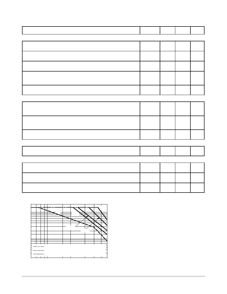
Figure 1. Power Derating
T
C
, CASE TEMPERATURE (
░
C)
P
D
, POWER DISSIP
A
TION (W
A
TTS)
140
120
100
80
60
40
20
15 A
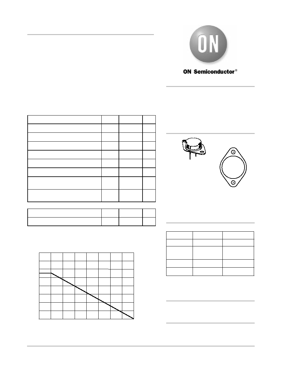
POWER TRANSISTORS
COMPLEMENTARY SILICON
60 V
115 W
http://onsemi.com
Preferred devices are recommended choices for future use
and best overall value.
Device
Package
Shipping
ORDERING INFORMATION
2N3055
TO-204AA
100 Units / Tray
MJ2955
TO-204AA
TO-204AA (TO-3)
CASE 1-07
100 Units / Tray
MARKING
DIAGRAM
xxxx55 = Device Code
xxxx= 2N3055 or MJ2955
A
= Assembly Location
YY
= Year
WW
= Work Week
x
= 1, 2, or 3
xxxx55
A
YYWW
2N3055G
TO-204AA
(Pb-Free)
1 Units / Tubes
2N3055H
TO-204AA
100 Units / Tray
For information on tape and reel specifications,
including part orientation and tape sizes, please
refer to our Tape and Reel Packaging Specifications
Brochure, BRD8011/D.
*For additional information on our Pb-Free strategy
and soldering details, please download the
ON Semiconductor Soldering and Mounting
Techniques Reference Manual, SOLDERRM/D.
2N3055, MJ2955
http://onsemi.com
2
ELECTRICAL CHARACTERISTICS
(T
C
= 25
░
C unless otherwise noted)
╬╬╬╬╬╬╬╬╬╬╬╬╬╬╬╬╬╬╬╬╬╬
╬
╬╬╬╬╬╬╬╬╬╬╬╬╬╬╬╬╬╬╬╬
╬
╬╬╬╬╬╬╬╬╬╬╬╬╬╬╬╬╬╬╬╬╬╬
Characteristic
╬╬╬╬╬
╬
╬╬╬
╬
╬╬╬╬╬
Symbol
╬╬╬
╬
╬
╬
╬╬╬
Min
╬╬╬╬
╬
╬╬
╬
╬╬╬╬
Max
╬╬╬
╬
╬
╬
╬╬╬
Unit
*OFF CHARACTERISTICS
Collector-Emitter Sustaining Voltage (Note 1)
(I
C
= 200 mAdc, I
B
= 0)
V
CEO(sus)
60
-
Vdc
Collector-Emitter Sustaining Voltage (Note 1)
(I
C
= 200 mAdc, R
BE
= 100
W
)
V
CER(sus)
70
-
Vdc
╬╬╬╬╬╬╬╬╬╬╬╬╬╬╬╬╬╬╬╬╬╬
╬
╬╬╬╬╬╬╬╬╬╬╬╬╬╬╬╬╬╬╬╬
╬
╬╬╬╬╬╬╬╬╬╬╬╬╬╬╬╬╬╬╬╬╬╬
Collector Cutoff Current
(V
CE
= 30 Vdc, I
B
= 0)
╬╬╬╬╬
╬
╬╬╬
╬
╬╬╬╬╬
I
CEO
╬╬╬
╬
╬
╬
╬╬╬
-
╬╬╬╬
╬
╬╬
╬
╬╬╬╬
0.7
╬╬╬
╬
╬
╬
╬╬╬
mAdc
╬╬╬╬╬╬╬╬╬╬╬╬╬╬╬╬╬╬╬╬╬╬
╬
╬╬╬╬╬╬╬╬╬╬╬╬╬╬╬╬╬╬╬╬
╬
╬╬╬╬╬╬╬╬╬╬╬╬╬╬╬╬╬╬╬╬╬╬
Collector Cutoff Current
(V
CE
= 100 Vdc, V
BE(off)
= 1.5 Vdc)
(V
CE
= 100 Vdc, V
BE(off)
= 1.5 Vdc, T
C
= 150
░
C)
╬╬╬╬╬
╬
╬╬╬
╬
╬╬╬╬╬
I
CEX
╬╬╬
╬
╬
╬
╬╬╬
-
-
╬╬╬╬
╬
╬╬
╬
╬╬╬╬
1.0
5.0
╬╬╬
╬
╬
╬
╬╬╬
mAdc
╬╬╬╬╬╬╬╬╬╬╬╬╬╬╬╬╬╬╬╬╬╬
╬
╬╬╬╬╬╬╬╬╬╬╬╬╬╬╬╬╬╬╬╬
╬
╬╬╬╬╬╬╬╬╬╬╬╬╬╬╬╬╬╬╬╬╬╬
Emitter Cutoff Current
(V
BE
= 7.0 Vdc, I
C
= 0)
╬╬╬╬╬
╬
╬╬╬
╬
╬╬╬╬╬
I
EBO
╬╬╬
╬
╬
╬
╬╬╬
-
╬╬╬╬
╬
╬╬
╬
╬╬╬╬
5.0
╬╬╬
╬
╬
╬
╬╬╬
mAdc
╬╬╬╬╬╬╬╬╬╬╬╬╬╬╬╬╬╬╬╬╬╬╬╬╬╬╬╬╬╬╬╬╬
╬╬╬╬╬╬╬╬╬╬╬╬╬╬╬╬╬╬╬╬╬╬╬╬╬╬╬╬╬╬╬╬╬
*ON CHARACTERISTICS (Note 1)
DC Current Gain
(I
C
= 4.0 Adc, V
CE
= 4.0 Vdc)
(I
C
= 10 Adc, V
CE
= 4.0 Vdc)
h
FE
20
5.0
70
-
-
Collector-Emitter Saturation Voltage
(I
C
= 4.0 Adc, I
B
= 400 mAdc)
(I
C
= 10 Adc, I
B
= 3.3 Adc)
V
CE(sat)
-
1.1
3.0
Vdc
Base-Emitter On Voltage
(I
C
= 4.0 Adc, V
CE
= 4.0 Vdc)
V
BE(on)
-
1.5
Vdc
╬╬╬╬╬╬╬╬╬╬╬╬╬╬╬╬╬╬╬╬╬╬╬╬╬╬╬╬╬╬╬╬╬
╬╬╬╬╬╬╬╬╬╬╬╬╬╬╬╬╬╬╬╬╬╬╬╬╬╬╬╬╬╬╬╬╬
SECOND BREAKDOWN
╬╬╬╬╬╬╬╬╬╬╬╬╬╬╬╬╬╬╬╬╬╬
╬
╬╬╬╬╬╬╬╬╬╬╬╬╬╬╬╬╬╬╬╬
╬
╬╬╬╬╬╬╬╬╬╬╬╬╬╬╬╬╬╬╬╬╬╬
Second Breakdown Collector Current with Base Forward Biased
(V
CE
= 40 Vdc, t = 1.0 s, Nonrepetitive)
╬╬╬╬╬
╬
╬╬╬
╬
╬╬╬╬╬
I
s/b
╬╬╬
╬
╬
╬
╬╬╬
2.87
╬╬╬╬
╬
╬╬
╬
╬╬╬╬
-
╬╬╬
╬
╬
╬
╬╬╬
Adc
╬╬╬╬╬╬╬╬╬╬╬╬╬╬╬╬╬╬╬╬╬╬╬╬╬╬╬╬╬╬╬╬╬
╬╬╬╬╬╬╬╬╬╬╬╬╬╬╬╬╬╬╬╬╬╬╬╬╬╬╬╬╬╬╬╬╬
DYNAMIC CHARACTERISTICS
╬╬╬╬╬╬╬╬╬╬╬╬╬╬╬╬╬╬╬╬╬╬
╬
╬╬╬╬╬╬╬╬╬╬╬╬╬╬╬╬╬╬╬╬
╬
╬╬╬╬╬╬╬╬╬╬╬╬╬╬╬╬╬╬╬╬╬╬
Current Gain - Bandwidth Product
(I
C
= 0.5 Adc, V
CE
= 10 Vdc, f = 1.0 MHz)
╬╬╬╬╬
╬
╬╬╬
╬
╬╬╬╬╬
f
T
╬╬╬
╬
╬
╬
╬╬╬
2.5
╬╬╬╬
╬
╬╬
╬
╬╬╬╬
-
╬╬╬
╬
╬
╬
╬╬╬
MHz
╬╬╬╬╬╬╬╬╬╬╬╬╬╬╬╬╬╬╬╬╬╬
╬
╬╬╬╬╬╬╬╬╬╬╬╬╬╬╬╬╬╬╬╬
╬
╬╬╬╬╬╬╬╬╬╬╬╬╬╬╬╬╬╬╬╬╬╬
*Small-Signal Current Gain
(I
C
= 1.0 Adc, V
CE
= 4.0 Vdc, f = 1.0 kHz)
╬╬╬╬╬
╬
╬╬╬
╬
╬╬╬╬╬
h
fe
╬╬╬
╬
╬
╬
╬╬╬
15
╬╬╬╬
╬
╬╬
╬
╬╬╬╬
120
╬╬╬
╬
╬
╬
╬╬╬
-
╬╬╬╬╬╬╬╬╬╬╬╬╬╬╬╬╬╬╬╬╬╬
╬╬╬╬╬╬╬╬╬╬╬╬╬╬╬╬╬╬╬╬╬╬
*Small-Signal Current Gain Cutoff Frequency
(V
CE
= 4.0 Vdc, I
C
= 1.0 Adc, f = 1.0 kHz)
╬╬╬╬╬
╬╬╬╬╬
f
hfe
╬╬╬
╬╬╬
10
╬╬╬╬
╬╬╬╬
-
╬╬╬
╬╬╬
kHz
*Indicates Within JEDEC Registration. (2N3055)
1. Pulse Test: Pulse Width
v
300
m
s, Duty Cycle
v
2.0%.
20
6
Figure 2. Active Region Safe Operating Area
V
CE
, COLLECTOR-EMITTER VOLTAGE (VOLTS)
10
6
4
2
1
0.6
0.4
0.2
10
20
40
60
I C
, COLLECT
OR CURRENT
(AMP)
dc
500 ms
1 ms
250 ms
50 ms
BONDING WIRE LIMIT
THERMALLY LIMITED @ T
C
= 25
░
C (SINGLE PULSE)
SECOND BREAKDOWN LIMIT
There are two limitations on the power handling ability of
a transistor: average junction temperature and second
breakdown. Safe operating area curves indicate I
C
- V
CE
limits of the transistor that must be observed for reliable
operation; i.e., the transistor must not be subjected to greater
dissipation than the curves indicate.
The data of Figure 2 is based on T
C
= 25
░
C; T
J(pk)
is
variable depending on power level. Second breakdown
pulse limits are valid for duty cycles to 10% but must be
derated for temperature according to Figure 1.

2N3055, MJ2955
http://onsemi.com
3
V CE
, COLLECT
OR-EMITTER VOL
T
AGE (VOL
TS)
V CE
, COLLECT
OR-EMITTER VOL
T
AGE (VOL
TS)
500
0.1
Figure 3. DC Current Gain, 2N3055 (NPN)
I
C
, COLLECTOR CURRENT (AMP)
5.0
0.2 0.3
0.5 0.7 1.0
2.0 3.0
5.0
10
100
50
30
20
200
70
h FE
, DC CURRENT
GAIN
T
J
= 150
░
C
25
░
C
-55
░
C
V
CE
= 4.0 V
200
0.1
I
C
, COLLECTOR CURRENT (AMP)
10
0.2
0.3
0.5 0.7 1.0
2.0 3.0
5.0
10
70
30
20
100
50
h FE
, DC CURRENT
GAIN
T
J
= 150
░
C
25
░
C
-55
░
C
V
CE
= 4.0 V
7.0
10
300
7.0
7.0
Figure 4. DC Current Gain, MJ2955 (PNP)
2.0
5.0
I
B
, BASE CURRENT (mA)
0
10
20
50
100
200
500
1000 2000
5000
1.6
1.2
0.8
0.4
I
C
= 1.0 A
T
J
= 25
░
C
4.0 A
8.0 A
2.0
I
B
, BASE CURRENT (mA)
0
1.6
1.2
0.8
0.4
1.4
0.1
I
C
, COLLECTOR CURRENT (AMPERES)
0.2 0.3
0.5 0.7 1.0
2.0
3.0
5.0
10
1.0
0.6
0.4
0.2
0
T
J
= 25
░
C
V
BE(sat)
@ I
C
/I
B
= 10
V
CE(sat)
@ I
C
/I
B
= 10
V
,
VOL
T
AGE (VOL
TS)
Figure 5. Collector Saturation Region,
2N3055 (NPN)
1.2
0.8
7.0
V
BE
@ V
CE
= 4.0 V
2.0
0.1
I
C
, COLLECTOR CURRENT (AMP)
0.2
0.3
0.5
1.0
2.0
3.0
5.0
10
1.2
0.4
0
T
J
= 25
░
C
V
BE(sat)
@ I
C
/I
B
= 10
V
CE(sat)
@ I
C
/I
B
= 10
V
,
VOL
T
AGE (VOL
TS)
1.6
0.8
V
BE
@ V
CE
= 4.0 V
5.0
10
20
50
100
200
500
1000 2000
5000
I
C
= 1.0 A
T
J
= 25
░
C
4.0 A
8.0 A
Figure 6. Collector Saturation Region,
MJ2955 (PNP)
Figure 7. "On" Voltages, 2N3055 (NPN)
Figure 8. "On" Voltages, MJ2955 (PNP)
2N3055, MJ2955
http://onsemi.com
4
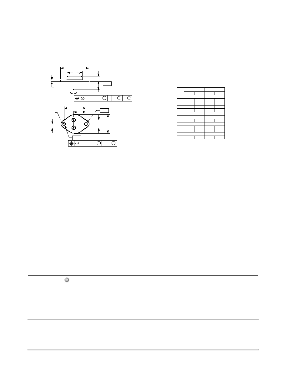
PACKAGE DIMENSIONS
NOTES:
1. DIMENSIONING AND TOLERANCING PER ANSI
Y14.5M, 1982.
2. CONTROLLING DIMENSION: INCH.
3. ALL RULES AND NOTES ASSOCIATED WITH
REFERENCED TO-204AA OUTLINE SHALL APPLY.
DIM
MIN
MAX
MIN
MAX
MILLIMETERS
INCHES
A
1.550 REF
39.37 REF
B
---
1.050
---
26.67
C
0.250
0.335
6.35
8.51
D
0.038
0.043
0.97
1.09
E
0.055
0.070
1.40
1.77
G
0.430 BSC
10.92 BSC
H
0.215 BSC
5.46 BSC
K
0.440
0.480
11.18
12.19
L
0.665 BSC
16.89 BSC
N
---
0.830
---
21.08
Q
0.151
0.165
3.84
4.19
U
1.187 BSC
30.15 BSC
V
0.131
0.188
3.33
4.77
A
N
E
C
K
-T-
SEATING
PLANE
2 PL
D
M
Q
M
0.13 (0.005)
Y
M
T
M
Y
M
0.13 (0.005)
T
-Q-
-Y-
2
1
U
L
G
B
V
H
TO-204 (TO-3)
CASE 1-07
ISSUE Z
ON Semiconductor and are registered trademarks of Semiconductor Components Industries, LLC (SCILLC). SCILLC reserves the right to make changes without further notice
to any products herein. SCILLC makes no warranty, representation or guarantee regarding the suitability of its products for any particular purpose, nor does SCILLC assume any liability
arising out of the application or use of any product or circuit, and specifically disclaims any and all liability, including without limitation special, consequential or incidental damages.
"Typical" parameters which may be provided in SCILLC data sheets and/or specifications can and do vary in different applications and actual performance may vary over time. All
operating parameters, including "Typicals" must be validated for each customer application by customer's technical experts. SCILLC does not convey any license under its patent rights
nor the rights of others. SCILLC products are not designed, intended, or authorized for use as components in systems intended for surgical implant into the body, or other applications
intended to support or sustain life, or for any other application in which the failure of the SCILLC product could create a situation where personal injury or death may occur. Should
Buyer purchase or use SCILLC products for any such unintended or unauthorized application, Buyer shall indemnify and hold SCILLC and its officers, employees, subsidiaries, affiliates,
and distributors harmless against all claims, costs, damages, and expenses, and reasonable attorney fees arising out of, directly or indirectly, any claim of personal injury or death
associated with such unintended or unauthorized use, even if such claim alleges that SCILLC was negligent regarding the design or manufacture of the part. SCILLC is an Equal
Opportunity/Affirmative Action Employer. This literature is subject to all applicable copyright laws and is not for resale in any manner.
PUBLICATION ORDERING INFORMATION
N. American Technical Support: 800-282-9855 Toll Free
USA/Canada
Japan: ON Semiconductor, Japan Customer Focus Center
2-9-1 Kamimeguro, Meguro-ku, Tokyo, Japan 153-0051
Phone: 81-3-5773-3850
2N3055/D
LITERATURE FULFILLMENT:
Literature Distribution Center for ON Semiconductor
P.O. Box 5163, Denver, Colorado 80217 USA
Phone: 303-675-2175 or 800-344-3860 Toll Free USA/Canada
Fax: 303-675-2176 or 800-344-3867 Toll Free USA/Canada
Email: orderlit@onsemi.com
ON Semiconductor Website: http://onsemi.com
Order Literature: http://www.onsemi.com/litorder
For additional information, please contact your
local Sales Representative.