©
Semiconductor Components Industries, LLC, 2004
March, 2004 - Rev. 3
1
Publication Order Number:
MDC3105LT1/D
MDC3105LT1
Integrated Relay,
Inductive Load Driver
This device is intended to replace an array of three to six discrete
components with an integrated SMT part. It is available in a SOT-23
package. It can be used to switch 3 to 6 Vdc inductive loads such as
relays, solenoids, incandescent lamps, and small DC motors without
the need of a free-wheeling diode.
·
Provides a Robust Driver Interface between D.C. Relay Coil and
Sensitive Logic Circuits
·
Optimized to Switch Relays from a 3 V to 5 V Rail
·
Capable of Driving Relay Coils Rated up to 2.5 W at 5 V
·
Features Low Input Drive Current & Good Back-to-Front Transient
Isolation
·
Internal Zener Eliminates Need for Free-Wheeling Diode
·
Internal Zener Clamp Routes Induced Current to Ground for Quieter
System Operation
·
Guaranteed Off State with No Input Connection
·
Supports Large Systems with Minimal Off-State Leakage
·
ESD Resistant in Accordance with the 2000 V Human Body Model
·
Low Sat Voltage Reduces System Current Drain by Allowing Use of
Higher Resistance Relay Coils
Applications Include:
·
Telecom: Line Cards, Modems, Answering Machines, FAX
Machines, Feature Phone Electronic Hook Switch
·
Computer & Office: Photocopiers, Printers, Desktop Computers
·
Consumer: TVs & VCRs, Stereo Receivers, CD Players, Cassette
Recorders, TV Set Top Boxes
·
Industrial: Small Appliances, White Goods, Security Systems,
Automated Test Equipment, Garage Door Openers
·
Automotive: 5.0 V Driven Relays, Motor Controls, Power Latches,
Lamp Drivers
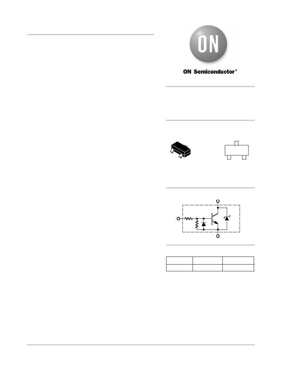
http://onsemi.com
Device
Package
Shipping
ORDERING INFORMATION
MDC3105LT1
SOT-23
3000 Units/Reel
MARKING
DIAGRAM
RELAY/INDUCTIVE
LOAD DRIVER
SILICON SMALLBLOCK
]
INTEGRATED CIRCUIT
1
2
3
SOT-23
(TO-236)
CASE 318
STYLE 6
INTERNAL CIRCUIT DIAGRAM
JW D
JW
= Specific Device Code
D
= Date Code
For information on tape and reel specifications,
including part orientation and tape sizes, please
refer to our Tape and Reel Packaging Specification
Brochure, BRD8011/D.
V
out
(3)
V
in
(1)
1.0 k
33 k
6.6 V
GND
(2)

MDC3105LT1
http://onsemi.com
2
MAXIMUM RATINGS
(T
J
= 25
°
C unless otherwise noted)
Rating
Symbol
Value
Unit
Power Supply Voltage
V
CC
6.0
Vdc
Input Voltage
V
in(fwd)
6.0
Vdc
Reverse Input Voltage
V
in(rev)
- 0.5
Vdc
Repetitive Pulse Zener Energy Limit (Duty Cycle
0.01%)
Ezpk
50
mJ
Output Sink Current
Continuous
I
O
500
mA
Junction Temperature
T
J
150
°
C
Operating Ambient Temperature Range
T
A
- 40 to +85
°
C
Storage Temperature Range
T
stg
- 65 to +150
°
C
THERMAL CHARACTERISTICS
Characteristic
Symbol
Value
Unit
Total Device Power Dissipation
(1)
Derate above 25
°
C
P
D
225
1.8
mW
mW/
°
C
Thermal Resistance Junction to Ambient
R
q
JA
556
°
C/W
1. FR-5 PCB of 1
x 0.75
x 0.062
, T
A
= 25
°
C
ELECTRICAL CHARACTERISTICS
(T
A
= 25
°
C unless otherwise noted)
Characteristic
Symbol
Min
Typ
Max
Unit
OFF CHARACTERISTICS
Output Zener Breakdown Voltage
V
(BRout)
6.2
6.6
7.0
V
(@ IT = 10 mA Pulse)
V
(-BRout)
--
- 0.7
--
V
Output Leakage Current @ 0 Input Voltage
(V
O
= 5.5 Vdc, V
in
= O.C., T
A
= 25
°
C)
(V
O
= 5.5 Vdc, V
in
= O.C., T
A
= 85
°
C)
I
OO
--
--
--
--
5.0
30
µ
A
Guaranteed "OFF" State Input Voltage (I
O
100
m
A)
V
in(off)
--
--
0.4
V
ON CHARACTERISTICS
Input Bias Current (H
FE
Limited)
(I
O
= 250 mA, V
O
= 0.25 Vdc)
I
in
--
0.8
1.6
mAdc
Output Saturation Voltage
(I
O
= 250 mA, I
in
= 1.5 mA)
V
O(sat)
--
0.12
0.16
Vdc
Output Sink Current
Continuous
(V
CE
= 0.25 Vdc, I
in
= 1.5 mA)
I
O(on)
250
400
--
mA

MDC3105LT1
http://onsemi.com
3
TYPICAL APPLICATION-DEPENDENT SWITCHING PERFORMANCE
SWITCHING CHARACTERISTICS
Characteristic
Symbol
Min
Typ
Max
Units
Propagation Delay Times:
High to Low Propagation Delay; Figure 1 (5.0 V 74HC04)
Low to High Propagation Delay; Figure 1 (5.0 V 74HC04)
High to Low Propagation Delay; Figures 1, 13 (3.0 V 74HC04)
Low to High Propagation Delay; Figures 1, 13 (3.0 V 74HC04)
High to Low Propagation Delay; Figures 1, 14 (5.0 V 74LS04)
Low to High Propagation Delay; Figures 1, 14 (5.0 V 74LS04)
t
PHL
t
PLH
t
PHL
t
PLH
t
PHL
t
PLH
--
--
--
--
--
--
55
430
85
315
55
2.4
--
--
--
--
--
--
nS
m
S
Transition Times:
Fall Time; Figure 1 (5.0 V 74HC04)
Rise Time; Figure 1 (5.0 V 74HC04)
Fall Time; Figures 1, 13 (3.0 V 74HC04)
Rise Time; Figures 1, 13 (3.0 V 74HC04)
Fall Time; Figures 1, 14 (5.0 V 74LS04)
Rise Time; Figures 1, 14 (5.0 V 74LS04)
t
f
t
r
t
f
t
r
t
f
t
r
--
--
--
--
--
--
45
160
70
195
45
2.4
--
--
--
--
--
--
nS
m
S
Figure 1. Switching Waveforms
V
out
GND
V
in
GND
V
Z
V
CC
V
CC
t
r
t
f
t
PLH
t
PHL
50%
90%
50%
10%
MDC3105LT1
http://onsemi.com
4
10 mA
50 mA
125 mA
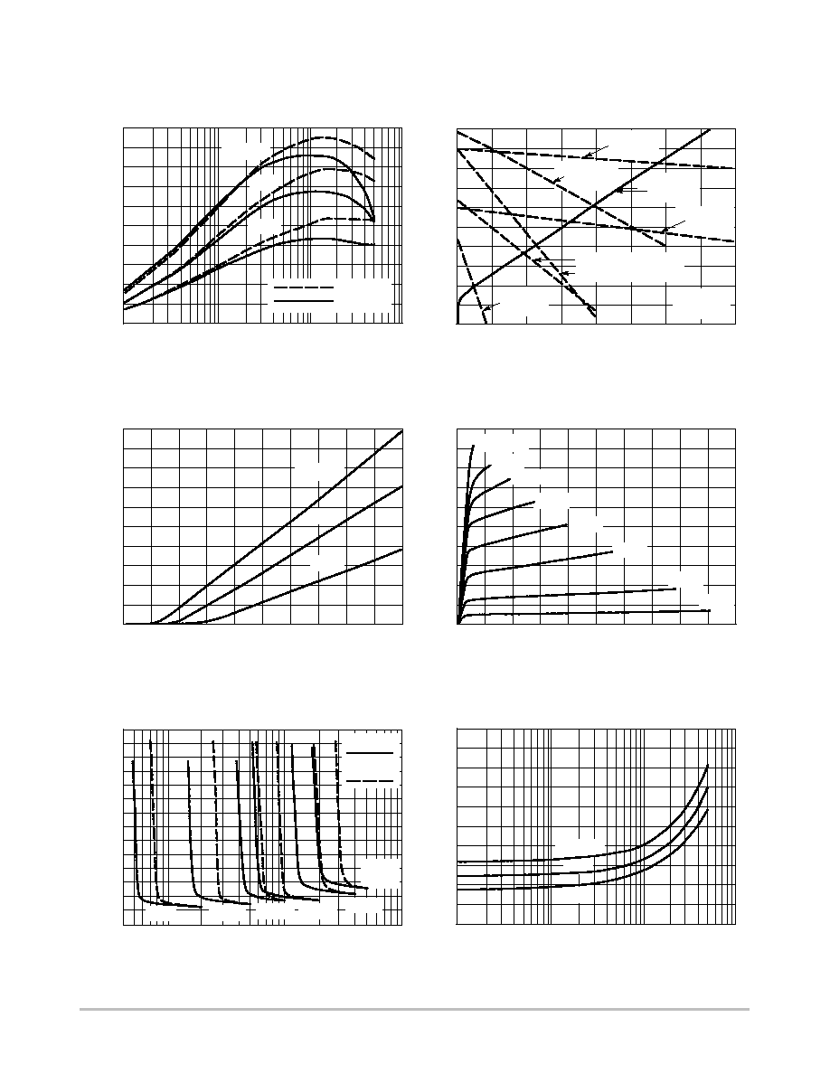
TYPICAL PERFORMANCE CHARACTERISTICS
(ON CHARACTERISTICS)
Figure 2. Transistor DC Current Gain
Figure 3. Input V-I Requirement Compared to
Possible Source Logic Outputs
Figure 4. Threshold Effects
Figure 5. Transistor Output V-I Characteristic
Figure 6. Output Saturation Voltage versus
I
t
/I
i
Figure 7. Zener Clamp Voltage versus Zener
C rrent
100
1000
1.0
I
O
, OUTPUT SINK CURRENT (mA)
350
300
200
250
150
INPUT CURRENT (mA)
2.5
4.0
0
2.0
1.0
0.5
0
0
INPUT CURRENT (mA)
50
10
5.0
0
V
O
, OUTPUT VOLTAGE (Vdc)
1.0
0
500
400
300
200
100
0
2.0
0.1
0.04
I
in
, INPUT CURRENT (mA)
1.3
0.3
0.2
0.1
0
I
Z
, ZENER CURRENT (mA)
1.0
100
8.5
8.0
7.5
6.5
6.0
10
H
FE
,
TRANSIST
OR DC CURRENT
GAIN
INPUT
VOL
T
AGE (VOL
TS)
OUTPUT
CURRENT
(mA)
I out
, OUTPUT
CURRENT
(mA)
100
50
0
10
3.0
3.5
0.5
1.0
1.5
2.0
1.5
2.5
3.0
0.01 0.02 0.03 0.04
0.05
0.5
3.0
1.5
4.0
4.5
5.0
, OUTPUT
VOL
T
AGE (Vdc)
V out
1.0
10
1000
7.0
V
Z
, ZENER CLAMP
VOL
T
AGE (VOL
TS)
500
400
450
4.0
3.5
4.5
5.0
0.06 0.07 0.08 0.09
0.1
20
15
30
25
40
35
45
2.5
3.5
0.6
0.5
0.4
0.9
0.8
0.7
1.2
1.1
1.0
T
J
= 85
°
C
25
°
C
-40
°
C
T
J
= 85
°
C
25
°
C
-40
°
C
I
in
= 1.5 mA
1.2 mA
1.0 mA
0.8 mA
0.6 mA
0.4 mA
0.2 mA
0.1 mA
T
J
= 85
°
C
25
°
C
-40
°
C
V
O
= 1.0 V
V
O
= 0.25 V
MC54LS04
+BAL99LT1
MDC3105LT1
V
in
vs. I
in
MC74HC04
@ 4.5 Vdc
MC68HC05C8
@ 5.0 Vdc
MC68HC05C8 @ 3.3 Vdc
MC14049B @ 4.5 Vdc
MC74HC04
@ 3.0 Vdc
T
J
= 25
°
C
V
O
= 0.25 V
I
out
=
500 mA
T
J
= 25
°
C
T
J
= -40
°
C
175 mA
350 mA
