ę
Semiconductor Components Industries, LLC, 1999
February, 2000 ş Rev. 1
1
Publication Order Number:
MCR68/D
MCR68-2
Silicon Controlled Rectifiers
Reverse Blocking Thyristors
Designed for overvoltage protection in crowbar circuits.
Ě
Glass-Passivated Junctions for Greater Parameter Stability and
Reliability
Ě
Center-Gate Geometry for Uniform Current Spreading Enabling
High Discharge Current
Ě
Small Rugged, Thermowatt Package Constructed for Low Thermal
Resistance and Maximum Power Dissipation and Durability
Ě
High Capacitor Discharge Current, 300 Amps
Ě
Device Marking: Logo, Device Type, e.g., MCR68ş2, Date Code
MAXIMUM RATINGS
(TJ = 25
░
C unless otherwise noted)
Rating
Symbol
Value
Unit
Peak Repetitive OffşState Voltage(1)
(TJ =
*
40 to +125
░
C, Gate Open)
MCR68ş2
VDRM,
VRRM
50
Volts
Peak Discharge Current(2)
ITM
300
Amps
On-State RMS Current
(180
░
Conduction Angles; TC = 85
░
C)
IT(RMS)
12
Amps
Average On-State Current
(180
░
Conduction Angles; TC = 85
░
C)
IT(AV)
8.0
Amps
Peak Non-Repetitive Surge Current
(1/2 Cycle, Sine Wave, 60 Hz,
TJ = 125
░
C)
ITSM
100
Amps
Circuit Fusing Considerations
(t = 8.3 ms)
I2t
40
A2s
Forward Peak Gate Current
(t
1.0
Á
s, TC = 85
░
C)
IGM
2.0
Amps
Forward Peak Gate Power
(t
1.0
Á
s, TC = 85
░
C)
PGM
20
Watts
Forward Average Gate Power
(t = 8.3 ms, TC = 85
░
C)
PG(AV)
0.5
Watt
Operating Junction Temperature Range
TJ
ş 40 to
+125
░
C
Storage Temperature Range
Tstg
ş 40 to
+150
░
C
Mounting Torque
--
8.0
in. lb.
(1) VDRM and VRRM for all types can be applied on a continuous basis. Ratings
apply for zero or negative gate voltage; however, positive gate voltage shall
not be applied concurrent with negative potential on the anode. Blocking
voltages shall not be tested with a constant current source such that the
voltage ratings of the devices are exceeded.
(2) Ratings apply for tw = 1 ms. See Figure 1 for ITM capability for various
duration of an exponentially decaying current waveform, tw is defined as
5 time constants of an exponentially decaying current pulse.
SCRs
12 AMPERES RMS
50 VOLTS
Device
Package
Shipping
ORDERING INFORMATION
MCR68ş2
TO220AB
500/Box
http://onsemi.com
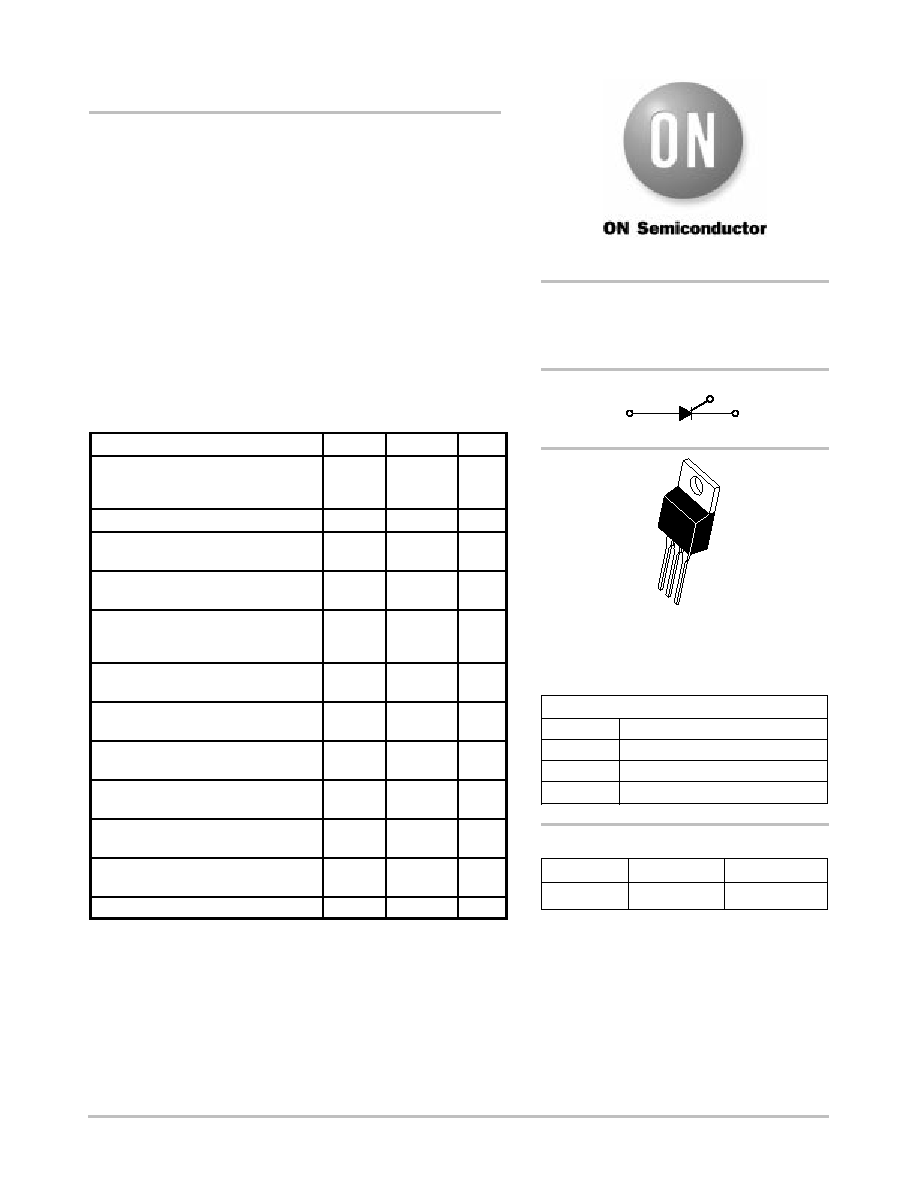
K
G
A
TOş220AB
CASE 221A
STYLE 3
1
2
3
4
PIN ASSIGNMENT
1
2
3
Anode
Gate
Cathode
4
Anode
MCR68ş2
http://onsemi.com
2
THERMAL CHARACTERISTICS
Characteristic
Symbol
Max
Unit
Thermal Resistance, Junction to Case
R
JC
2.0
░
C/W
Thermal Resistance, Junction to Ambient
R
JA
60
░
C/W
Maximum Lead Temperature for Soldering Purposes 1/8
from Case for 10 Seconds
TL
260
░
C
ELECTRICAL CHARACTERISTICS
(TC = 25
░
C unless otherwise noted.)
Characteristic
Symbol
Min
Typ
Max
Unit
OFF CHARACTERISTICS
Peak Repetitive Forward or Reverse Blocking Current
(VAK = Rated VDRM or VRRM, Gate Open)
TJ = 25
░
C
TJ = 125
░
C
IDRM, IRRM
--
--
--
--
10
2.0
Á
A
mA
ON CHARACTERISTICS
Peak Forward On-State Voltage
(ITM = 24 A)(1)
(ITM = 300 A, tw = 1 ms)(2)
VTM
--
--
--
6.0
2.2
--
Volts
Gate Trigger Current (Continuous dc)
(VD = 12 V, RL = 100
)
IGT
2.0
7.0
30
mA
Gate Trigger Voltage (Continuous dc)
(VD = 12 V, RL = 100
)
VGT
--
0.65
1.5
Volts
Gate NonşTrigger Voltage
(VD = 12 Vdc, RL = 100
, TJ = 125
░
C)
VGD
0.2
0.40
--
Volts
Holding Current
(VD = 12 V, Initiating Current = 200 mA, Gate Open)
IH
3.0
15
50
mA
Latching Current
(VD = 12 Vdc, IG = 150 mA)
IL
--
--
60
mA
Gate Controlled Turn-On Time(3)
(VD = Rated VDRM, IG = 150 mA)
(ITM = 24 A Peak)
tgt
--
1.0
--
Á
s
DYNAMIC CHARACTERISTICS
Critical Rate-of-Rise of Off-State Voltage
(VD = Rated VDRM, Gate Open, Exponential Waveform, TJ = 125
░
C)
dv/dt
10
--
--
V/
Á
s
Critical Rate-of-Rise of On-State Current
IG = 150 mA
TJ = 125
░
C
di/dt
--
--
75
A/
Á
s
(1) Pulse duration
p
300
Á
s, duty cycle
p
2%.
(2) Ratings apply for tw = 1 ms. See Figure 1 for ITM capability for various durations of an exponentially decaying current waveform. tw is defined
as 5 time constants of an exponentially decaying current pulse.
(3) The gate controlled turn-on time in a crowbar circuit will be influenced by the circuit inductance.

MCR68ş2
http://onsemi.com
3
+ Current
+ Voltage
VTM
IDRM at VDRM
IH
Symbol
Parameter
VDRM
Peak Repetitive Off State Forward Voltage
IDRM
Peak Forward Blocking Current
VRRM
Peak Repetitive Off State Reverse Voltage
IRRM
Peak Reverse Blocking Current
VTM
Peak On State Voltage
IH
Holding Current
Voltage Current Characteristic of SCR
Anode +
on state
Reverse Blocking Region
(off state)
Reverse Avalanche Region
Anode ş
Forward Blocking Region
IRRM at VRRM
(off state)
I , PEAK DISCHARGE CURRENT
(AMPS)
TM
NORMALIZED PEAK CURRENT
300
20
50
100
200
20
1000
0.5
50
tw, PULSE CURRENT DURATION (ms)
2.0
1.0
tw
tw = 5 time constants
ITM
10
5.0
0.8
25
0
0.2
0.4
0.6
1.0
50
75
100
125
TC, CASE TEMPERATURE (
░
C)
Figure 1. Peak Capacitor Discharge Current
Figure 2. Peak Capacitor Discharge Current
Derating
T
, MAXIMUM C
CASE
TEMPERA
TURE ( C)
░
75
80
85
90
95
100
105
110
115
120
125
5.0
2.0
1.0
8.0
10
IT(AV), AVERAGE ON-STATE CURRENT (AMPS)
dc
Half Wave
Figure 3. Current Derating
P
,
A
VERAGE
POWER
DISSIP
A
TION
(W
A
TTS)
(A
V) 2.0
4.0
8.0
10
14
18
20
Half Wave
dc
5.0
2.0
1.0
8.0
10
4.0
IT(AV), AVERAGE ON-STATE CURRENT (AMPS)
TJ = 125
░
C
Figure 4. Maximum Power Dissipation
MCR68ş2
http://onsemi.com
4
2 k
10 k
5 k
3 k
10
t, TIME (ms)
1 k
500
300
200
100
50
30
0.2
20
1
0.7
0.5
0.1
0.2
0.02
5
2
3
1
0.5
0.3
0.1
0.3
0.07
0.05
0.03
0.01
Z
JC(t) = R
JC
Ě
r(t)
r(t), TRANSIENT
THERMAL
RESIST
ANCE
(NORMALIZED)
Figure 5. Thermal Response
NORMALIZED GA
TE
TRIGGER
CURRENT
NORMALIZED GA
TE
TRIGGER
VOL
T
AGE
NORMALIZED HOLD CURRENT
ş40
10
0.2
0.3
140
120
100
80
60
40
ş20
0
20
0.5
1.2
1.0
0.8
ş40
ş60
1.4
TJ, JUNCTION TEMPERATURE (
░
C)
40
0
20
60
0.5
3.0
5.0
140
80
100
120
2.0
1.0
ş20
ş60
TJ, JUNCTION TEMPERATURE (
░
C)
VD = 12 Volts
RL = 100
VD = 12 Volts
RL = 100
0.3
0.5
0.8
1.0
140
120
40
100
3.0
2.0
20
60
80
0
ş40
TJ, JUNCTION TEMPERATURE (
░
C)
ş20
ş60
VD = 12 Volts
ITM = 100 mA
Figure 6. Gate Trigger Current
Figure 7. Gate Trigger Voltage
Figure 8. Holding Current

MCR68ş2
http://onsemi.com
5
PACKAGE DIMENSIONS
TOş220AB
CASE 221Aş07
ISSUE Z
NOTES:
1. DIMENSIONING AND TOLERANCING PER ANSI
Y14.5M, 1982.
2. CONTROLLING DIMENSION: INCH.
3. DIMENSION Z DEFINES A ZONE WHERE ALL
BODY AND LEAD IRREGULARITIES ARE
ALLOWED.
DIM
MIN
MAX
MIN
MAX
MILLIMETERS
INCHES
A
0.570
0.620
14.48
15.75
B
0.380
0.405
9.66
10.28
C
0.160
0.190
4.07
4.82
D
0.025
0.035
0.64
0.88
F
0.142
0.147
3.61
3.73
G
0.095
0.105
2.42
2.66
H
0.110
0.155
2.80
3.93
J
0.014
0.022
0.36
0.55
K
0.500
0.562
12.70
14.27
L
0.045
0.060
1.15
1.52
N
0.190
0.210
4.83
5.33
Q
0.100
0.120
2.54
3.04
R
0.080
0.110
2.04
2.79
S
0.045
0.055
1.15
1.39
T
0.235
0.255
5.97
6.47
U
0.000
0.050
0.00
1.27
V
0.045
şşş
1.15
şşş
Z
şşş
0.080
şşş
2.04
A
K
L
V
G
D
N
Z
H
Q
F
B
1
2
3
4
şTş
SEATING
PLANE
S
R
J
U
T
C
STYLE 3:
PIN 1. CATHODE
2. ANODE
3. GATE
4. ANODE