ˋ
Semiconductor Components Industries, LLC, 1999
November, 1999 Ù Rev. 1
1
Publication Order Number:
MC74VHC1G14/D
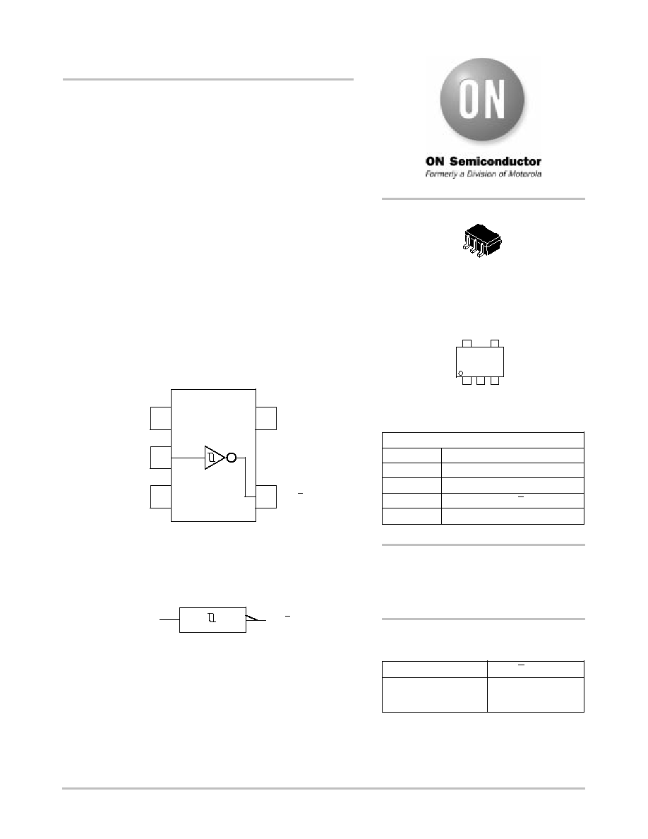
MC74VHC1G14
Schmitt-Trigger Inverter
The MC74VHC1G14 is a single gate CMOS SchmittÙtrigger
inverter fabricated with silicon gate CMOS technology. It achieves
high speed operation similar to equivalent Bipolar Schottky TTL
while maintaining CMOS low power dissipation.
The internal circuit is composed of three stages, including a buffer
output which provides high noise immunity and stable output.
The MC74VHC1G14 input structure provides protection when
voltages up to 7V are applied, regardless of the supply voltage. This
allows the MC74VHC1G14 to be used to interface 5V circuits to 3V
circuits.
The MC74VHC1G14 can be used to enhance noise immunity or to
square up slowly changing waveforms.
ñ
High Speed: tPD = 4.0ns (Typ) at VCC = 5V
ñ
Low Power Dissipation: ICC = 2
ç
A (Max) at TA = 25
¯
C
ñ
Power Down Protection Provided on Inputs
ñ
Balanced Propagation Delays
ñ
Pin and Function Compatible with Other Standard Logic Families
ñ
Latchup Performance Exceeds 300mA
Figure 1. 5ÙLead SOTÙ353 Pinout (Top View)
5
1
2
4
3
VCC
NC
IN A
OUT Y
GND
LOGIC SYMBOL
IN A
OUT Y
SCÙ88A / SOTÙ353
DF SUFFIX
CASE 419A
PIN ASSIGNMENT
1
2
3
GND
NC
IN A
http://onsemi.com
Pin 1
d = Date Code
VAd
4
5
VCC
OUT Y
FUNCTION TABLE
MARKING DIAGRAM
See detailed ordering and shipping information in the package
dimensions section on page 4 of this data sheet.
ORDERING INFORMATION
L
H
A Input
Y Output
H
L
MC74VHC1G14
http://onsemi.com
2
MAXIMUM RATINGS*
Characteristics
Symbol
Value
Unit
DC Supply Voltage
VCC
Ù0.5 to +7.0
V
DC Input Voltage
VIN
Ù0.5 to +7.0
V
DC Output Voltage
VCC = 0
High or Low State
VOUT
Ù0.5 to 7.0
Ù0.5 to VCC + 0.5
V
Input Diode Current
IIK
Ù20
mA
Output Diode Current
(VOUT < GND; VOUT > VCC)
IOK
+20
mA
DC Output Current, per Pin
IOUT
+25
mA
DC Supply Current, VCC and GND
ICC
+50
mA
Power dissipation in still air, SCÙ88A
PD
200
mW
Lead temperature, 1 mm from case for 10 s
TL
260
¯
C
Storage temperature
Tstg
Ù65 to +150
¯
C
* Maximum Ratings are those values beyond which damage to the device may occur. Exposure to these conditions or conditions beyond those
indicated may adversely affect device reliability. Functional operation under absoluteÙmaximumÙrated conditions is not implied. Functional
operation should be restricted to the Recommended Operating Conditions.
Derating -- SCÙ88A Package: Ù3 mW/
_
C from 65
_
to 125
_
C
RECOMMENDED OPERATING CONDITIONS
Characteristics
Symbol
Min
Max
Unit
DC Supply Voltage
VCC
4.5
5.5
V
DC Input Voltage
VIN
0.0
5.5
V
DC Output Voltage
VOUT
0.0
VCC
V
Operating Temperature Range
TA
Ù55
+85
¯
C
MC74VHC1G14
http://onsemi.com
3
DC ELECTRICAL CHARACTERISTICS
VCC
TA = 25
¯
C
TA
85
¯
C
TA
125
¯
C
Symbol
Parameter
Test Conditions
(V)
Min
Typ
Max
Min
Max
Min
Max
Unit
VT+
Positive Threshold
Voltage
3.0
4.5
5.5
1.85
2.86
3.50
2.0
3.0
3.6
2.20
3.15
3.85
2.20
3.15
3.85
2.20
3.15
3.85
V
VTÙ
Negative Threshold
Voltage
3.0
4.5
5.5
0.9
1.35
1.65
1.5
2.3
2.9
1.65
2.46
3.05
0.9
1.35
1.65
0.9
1.35
1.65
V
VH
Hysteresis Voltage
3.0
4.5
5.5
0.30
0.40
0.50
0.57
0.67
0.74
1.20
1.40
1.60
0.30
0.40
0.50
1.20
1.40
1.60
0.30
0.40
0.50
1.20
1.40
1.60
V
VOH
Minimum HighÙLevel
Output Voltage
IOH = Ù50
ç
A
VIN = VIH or VIL
IOH = Ù50
ç
A
2.0
3.0
4.5
1.9
2.9
4.4
2.0
3.0
4.5
1.9
2.9
4.4
1.9
2.9
4.4
V
IOH = Ù4mA
IOH = Ù8mA
3.0
4.5
2.58
3.94
2.48
3.80
2.34
3.66
V
VOL
Maximum LowÙLevel
Output Voltage
VIN = VIH or VIL
IOL = 50
ç
A
2.0
3.0
4.5
0.0
0.0
0.0
0.1
0.1
0.1
0.1
0.1
0.1
0.1
0.1
0.1
V
IOL = 4mA
IOL = 8mA
3.0
4.5
0.36
0.36
0.44
0.44
0.52
0.52
V
IIN
Maximum Input
Leakage Current
VIN = 5.5V or GND
0 to
5.5
Ý
0.1
Ý
1.0
Ý
1.0
ç
A
ICC
Maximum Quiescent
Supply Current
VIN = VCC or GND
5.5
2.0
20
40
ç
A
ööööööööööööööööööööööööööööööööö
ööööööööööööööööööööööööööööööööö
AC ELECTRICAL CHARACTERISTICS
(Cload = 50 pF, Input tr/tf = 3.0ns)
öööö
öööö
ööööööö
ööööööö
ööööööööö
ööööööööö
ööööööö
ööööööö
TA = 25
¯
C
ööööö
ööööö
TA
85
¯
C
ööööö
ööööö
TA
125
¯
C
öö
öö
öööö
öööö
Symbol
ööööööö
ööööööö
Parameter
ööööööööö
ööööööööö
Test Conditions
ööö
ööö
Min
ööö
ööö
Typ
ööö
ööö
Max
ööö
ööö
Min
ööö
ööö
Max
ööö
ööö
Min
ööö
ööö
Max
öö
öö
Unit
öööö
ö
öö
ö
öööö
tPLH,
tPHL
ööööööö
ö
ööööö
ö
ööööööö
Maximum
Propogation Delay,
A to Y
ööööööööö
ö
ööööööö
ö
ööööööööö
VCC = 3.3
Ý
0.3V
CL = 15 pF
CL = 50 pF
ööö
ö
ö
ö
ööö
ööö
ö
ö
ö
ööö
7.0
8.5
ööö
ö
ö
ö
ööö
12.8
16.3
ööö
ö
ö
ö
ööö
1.0
1.0
ööö
ö
ö
ö
ööö
15.0
18.5
ööö
ö
ö
ö
ööö
1.0
1.0
ööö
ö
ö
ö
ööö
17.0
20.5
öö
öö
öö
ns
öööö
ö
öö
ö
öööö
ööööööö
ö
ööööö
ö
ööööööö
A to Y
ööööööööö
ö
ööööööö
ö
ööööööööö
VCC = 5.0
Ý
0.5V
CL = 15 pF
CL = 50 pF
ööö
ö
ö
ö
ööö
ööö
ö
ö
ö
ööö
4.0
5.5
ööö
ö
ö
ö
ööö
8.6
10.6
ööö
ö
ö
ö
ööö
1.0
1.0
ööö
ö
ö
ö
ööö
10.0
12.0
ööö
ö
ö
ö
ööö
1.0
1.0
ööö
ö
ö
ö
ööö
11.5
13.5
öö
öö
öö
öööö
öööö
CIN
ööööööö
ööööööö
Maximum Input
Capacitance
ööööööööö
ööööööööö
ööö
ööö
ööö
ööö
5
ööö
ööö
10
ööö
ööö
ööö
ööö
10
ööö
ööö
ööö
ööö
10
öö
öö
pF
Typical @ 25
¯
C, VCC = 5.0V
CPD
Power Dissipation Capacitance (Note 1.)
7.0
pF
1. CPD is defined as the value of the internal equivalent capacitance which is calculated from the operating current consumption without load.
Average operating current can be obtained by the equation: ICC(OPR
)
= CPD
VCC
fin + ICC. CPD is used to determine the noÙload dynamic
power consumption; PD = CPD
VCC2
fin + ICC
VCC.

MC74VHC1G14
http://onsemi.com
4
VCC
GND
50%
50% VCC
A or B
Y
tPHL
tPLH
*Includes all probe and jig capacitance
CL*
TEST POINT
DEVICE
UNDER
TEST
OUTPUT
Figure 2. Switching Waveforms
Figure 3. Test Circuit
DEVICE ORDERING INFORMATION
Device Nomenclature
Device Order Number
Circuit
Indicator
Temp
Range
Identifier
Technology
Device
Function
Package
Suffix
Tape &
Reel
Suffix
Package
Type
Tape and Reel
Size
MC74VHC1G14DFT1
MC
74
VHC1G
14
DF
T1
SCÙ88A /
SOTÙ353
7ÙInch/3000 Unit
PACKAGE DIMENSIONS
NOTES:
1. DIMENSIONING AND TOLERANCING PER ANSI
Y14.5M, 1982.
2. CONTROLLING DIMENSION: MM.
DIM
A
MIN
MAX
MIN
MAX
MILLIMETERS
1.80
2.20
0.071
0.087
INCHES
B
1.15
1.35
0.045
0.053
C
0.80
1.10
0.031
0.043
D
0.10
0.30
0.004
0.012
G
0.65 BSC
0.026 BSC
H
ÙÙÙ
0.10
ÙÙÙ
0.004
J
0.10
0.25
0.004
0.010
K
0.10
0.30
0.004
0.012
N
0.20 REF
0.008 REF
S
2.00
2.20
0.079
0.087
V
0.30
0.40
0.012
0.016
B
0.2 (0.008)
M
M
1
2
3
4
5
A
G
V
S
D
5 PL
H
C
N
J
K
ÙBÙ
èèè
èèè
èèè
èèè
èèè
èèè
èèè
èèè
èèè
èèè
èèè
èèè
0.5 mm (min)
0.4 mm (min)
0.65 mm
0.65 mm
1.9 mm
SCÙ88A / SOTÙ353
DF SUFFIX
5ÙLEAD PACKAGE
CASE 419AÙ01
ISSUE B

MC74VHC1G14
http://onsemi.com
5
Figure 4. Carrier Tape Specifications
D1
FOR COMPONENTS
10 PITCHES
CUMULATIVE
TOLERANCE ON
TAPE
Ý
0.2 mm
(
Ý
0.008")
2.0 mm
æ
1.2 mm
AND LARGER
CENTER LINES
OF CAVITY
EMBOSSMENT
USER DIRECTION OF FEED
K0
SEE
NOTE 2
P0
P2
D
E
F
W
B0
+
+
+
K
t
B1
TOP
COVER
TAPE
P
SEE NOTE 2
A0
FOR MACHINE REFERENCE
ONLY
INCLUDING DRAFT AND RADII
CONCENTRIC AROUND B0
R MIN.
TAPE AND COMPONENTS
SHALL PASS AROUND RADIUS "R"
WITHOUT DAMAGE
BENDING RADIUS
*TOP COVER
TAPE THICKNESS (t1)
0.10 mm
(0.004") MAX.
EMBOSSED
CARRIER
EMBOSSMENT
TYPICAL
COMPONENT CAVITY
CENTER LINE
TYPICAL
COMPONENT
CENTER LINE
MAXIMUM COMPONENT ROTATION
10
¯
CAMBER (TOP VIEW)
ALLOWABLE CAMBER TO BE 1 mm/100 mm NONACCUMULATIVE OVER 250
mm
100 mm
(3.937")
1 mm
(0.039") MAX
250 mm
(9.843")
1 mm MAX
TAPE
EMBOSSED CARRIER DIMENSIONS (See Notes 1 and 2)
Tape
Size
B1
Max
D
D1
E
F
K
P
P0
P2
R
T
W
8 mm
4.35 mm
(0.171")
1.5 +0.1/
Ù0.0 mm
(0.059
+0.004/
Ù0.0")
1.0 mm
Min
(0.039")
1.75
Ý
0.1 mm
(0.069
Ý
0.004")
3.5
Ý
0.5 mm
(1.38
Ý
0.002")
2.4 mm
(0.094")
4.0
Ý
0.10 mm
(0.157
Ý
0.004")
4.0
Ý
0.1 mm
(0.156
Ý
0.004")
2.0
Ý
0.1 mm
(0.079
Ý
0.002")
25 mm
(0.98")
0.3
Ý
0.05 mm
(0.01
+0.0038/
Ù0.0002")
8.0
Ý
0.3 mm
(0.315
Ý
0.012")
1. Metric Dimensions GovernÙEnglish are in parentheses for reference only.
2. A0, B0, and K0 are determined by component size. The clearance between the components and the cavity must be within 0.05 mm min to
0.50 mm max. The component cannot rotate more than 10
¯
within the determined cavity