Äîêóìåíòàöèÿ è îïèñàíèÿ www.docs.chipfind.ru
©
Semiconductor Components Industries, LLC, 2000
March, 2000 Rev. 2
1
Publication Order Number:
MC74HCU04A/D
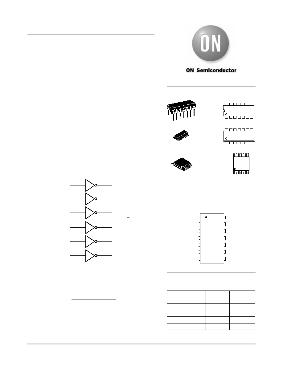
MC74HCU04A
Hex Unbuffered Inverter
HighPerformance SiliconGate CMOS
The MC74HCU04A is identical in pinout to the LS04 and the
MC14069UB. The device inputs are compatible with standard CMOS
outputs; with pullup resistors, they are compatible with LSTTL
outputs.
This device consists of six singlestage inverters. These inverters
are well suited for use as oscillators, pulse shapers, and in many other
applications requiring a highinput impedance amplifier. For digital
applications, the HC04A is recommended.
·
Output Drive Capability: 10 LSTTL Loads
·
Outputs Directly Interface to CMOS, NMOS, and TTL
·
Operating Voltage Range: 2 to 6 V; 2.5 to 6 V in Oscillator
Configurations
·
Low Input Current: 1
µ
A
·
High Noise Immunity Characteristic of CMOS Devices
·
In Compliance with the Requirements Defined by JEDEC Standard
No. 7A
·
Chip Complexity: 12 FETs or 3 Equivalent Gates
LOGIC DIAGRAM
Y1
A1
A2
A3
A4
A5
A6
Y2
Y3
Y4
Y5
Y6
1
3
5
9
11
13
2
4
6
8
10
12
Y = A
PIN 14 = VCC
PIN 7 = GND
FUNCTION TABLE
Inputs
A
L
H
Outputs
Y
H
L
Device
Package
Shipping
ORDERING INFORMATION
MC74HCU04AN
PDIP14
2000 / Box
MC74HCU04AD
SOIC14
http://onsemi.com
55 / Rail
MC74HCU04ADR2
SOIC14
2500 / Reel
MARKING
DIAGRAMS
A
= Assembly Location
WL or L
= Wafer Lot
YY or Y
= Year
WW or W = Work Week
MC74HCU04ADT
TSSOP14
96 / Rail
MC74HCU04ADTR2
TSSOP14
2500 / Reel
TSSOP14
DT SUFFIX
CASE 948G
HCU
04A
ALYW
1
14
1
14
PDIP14
N SUFFIX
CASE 646
MC74HCU04AN
AWLYYWW
SOIC14
D SUFFIX
CASE 751A
1
14
HCU04A
AWLYWW
PIN ASSIGNMENT
11
12
13
14
8
9
10
5
4
3
2
1
7
6
Y5
A5
Y6
A6
VCC
Y4
A4
Y2
A2
Y1
A1
GND
Y3
A3
MC74HCU04A
http://onsemi.com
2
ÎÎÎÎÎÎÎÎÎÎÎÎÎÎÎÎÎÎÎÎÎÎÎ
ÎÎÎÎÎÎÎÎÎÎÎÎÎÎÎÎÎÎÎÎÎÎÎ
MAXIMUM RATINGS*
ÎÎÎÎ
ÎÎÎÎ
Symbol
ÎÎÎÎÎÎÎÎÎÎÎÎÎÎ
ÎÎÎÎÎÎÎÎÎÎÎÎÎÎ
Parameter
ÎÎÎÎÎ
ÎÎÎÎÎ
Value
ÎÎÎ
ÎÎÎ
Unit
ÎÎÎÎ
ÎÎÎÎ
VCC
ÎÎÎÎÎÎÎÎÎÎÎÎÎÎ
ÎÎÎÎÎÎÎÎÎÎÎÎÎÎ
DC Supply Voltage (Referenced to GND)
ÎÎÎÎÎ
ÎÎÎÎÎ
0.5 to + 7.0
ÎÎÎ
ÎÎÎ
V
ÎÎÎÎ
ÎÎÎÎ
Vin
ÎÎÎÎÎÎÎÎÎÎÎÎÎÎ
ÎÎÎÎÎÎÎÎÎÎÎÎÎÎ
DC Input Voltage (Referenced to GND)
ÎÎÎÎÎ
ÎÎÎÎÎ
0.5 to VCC + 0.5
ÎÎÎ
ÎÎÎ
V
ÎÎÎÎ
ÎÎÎÎ
Vout
ÎÎÎÎÎÎÎÎÎÎÎÎÎÎ
ÎÎÎÎÎÎÎÎÎÎÎÎÎÎ
DC Output Voltage (Referenced to GND)
ÎÎÎÎÎ
ÎÎÎÎÎ
0.5 to VCC + 0.5
ÎÎÎ
ÎÎÎ
V
ÎÎÎÎ
ÎÎÎÎ
Iin
ÎÎÎÎÎÎÎÎÎÎÎÎÎÎ
ÎÎÎÎÎÎÎÎÎÎÎÎÎÎ
DC Input Current, per Pin
ÎÎÎÎÎ
ÎÎÎÎÎ
±
20
ÎÎÎ
ÎÎÎ
mA
ÎÎÎÎ
ÎÎÎÎ
Iout
ÎÎÎÎÎÎÎÎÎÎÎÎÎÎ
ÎÎÎÎÎÎÎÎÎÎÎÎÎÎ
DC Output Current, per Pin
ÎÎÎÎÎ
ÎÎÎÎÎ
±
25
ÎÎÎ
ÎÎÎ
mA
ÎÎÎÎ
ÎÎÎÎ
ICC
ÎÎÎÎÎÎÎÎÎÎÎÎÎÎ
ÎÎÎÎÎÎÎÎÎÎÎÎÎÎ
DC Supply Current, VCC and GND Pins
ÎÎÎÎÎ
ÎÎÎÎÎ
±
50
ÎÎÎ
ÎÎÎ
mA
ÎÎÎÎ
Î
ÎÎ
Î
ÎÎÎÎ
PD
ÎÎÎÎÎÎÎÎÎÎÎÎÎÎ
Î
ÎÎÎÎÎÎÎÎÎÎÎÎ
Î
ÎÎÎÎÎÎÎÎÎÎÎÎÎÎ
Power Dissipation in Still Air
Plastic DIP
SOIC Package
TSSOP Package
ÎÎÎÎÎ
Î
ÎÎÎ
Î
ÎÎÎÎÎ
750
500
450
ÎÎÎ
Î
Î
Î
ÎÎÎ
mW
ÎÎÎÎ
ÎÎÎÎ
Tstg
ÎÎÎÎÎÎÎÎÎÎÎÎÎÎ
ÎÎÎÎÎÎÎÎÎÎÎÎÎÎ
Storage Temperature
ÎÎÎÎÎ
ÎÎÎÎÎ
65 to + 150
ÎÎÎ
ÎÎÎ
_
C
ÎÎÎÎ
Î
ÎÎ
Î
ÎÎÎÎ
TL
ÎÎÎÎÎÎÎÎÎÎÎÎÎÎ
Î
ÎÎÎÎÎÎÎÎÎÎÎÎ
Î
ÎÎÎÎÎÎÎÎÎÎÎÎÎÎ
Lead Temperature, 1 mm from case for 10 Seconds
Plastic DIP, SOIC or TSSOP Package
ÎÎÎÎÎ
Î
ÎÎÎ
Î
ÎÎÎÎÎ
260
ÎÎÎ
Î
Î
Î
ÎÎÎ
_
C
*Maximum Ratings are those values beyond which damage to the device may occur.
Functional operation should be restricted to the Recommended Operating Conditions.
Derating -- Plastic DIP: 10mW/
_
C from 65
_
to 125
_
C
SOIC Package: 7mW/
_
C from 65
_
to 125
_
C
TSSOP Package: 6.1 mW/
_
C from 65
_
to 125
_
C
For high frequency or heavy load considerations, see Chapter 2 of the ON Semiconductor HighSpeed CMOS Data Book (DL129/D).
RECOMMENDED OPERATING CONDITIONS
ÎÎÎÎ
ÎÎÎÎ
Symbol
ÎÎÎÎÎÎÎÎÎÎÎÎÎÎÎ
ÎÎÎÎÎÎÎÎÎÎÎÎÎÎÎ
Parameter
ÎÎÎ
ÎÎÎ
Min
ÎÎ
ÎÎ
Max
ÎÎÎ
ÎÎÎ
Unit
ÎÎÎÎ
ÎÎÎÎ
VCC
ÎÎÎÎÎÎÎÎÎÎÎÎÎÎÎ
ÎÎÎÎÎÎÎÎÎÎÎÎÎÎÎ
DC Supply Voltage (Referenced to GND)
ÎÎÎ
ÎÎÎ
2.0
ÎÎ
ÎÎ
6.0
ÎÎÎ
ÎÎÎ
V
ÎÎÎÎ
ÎÎÎÎ
Vin, Vout
ÎÎÎÎÎÎÎÎÎÎÎÎÎÎÎ
ÎÎÎÎÎÎÎÎÎÎÎÎÎÎÎ
DC Input Voltage, Output Voltage (Referenced to GND)
ÎÎÎ
ÎÎÎ
0
ÎÎ
ÎÎ
VCC
ÎÎÎ
ÎÎÎ
V
ÎÎÎÎ
ÎÎÎÎ
TA
ÎÎÎÎÎÎÎÎÎÎÎÎÎÎÎ
ÎÎÎÎÎÎÎÎÎÎÎÎÎÎÎ
Operating Temperature, All Package Types
ÎÎÎ
ÎÎÎ
55
ÎÎ
ÎÎ
+ 125
ÎÎÎ
ÎÎÎ
_
C
ÎÎÎÎ
ÎÎÎÎ
tr, tf
ÎÎÎÎÎÎÎÎÎÎÎÎÎÎÎ
ÎÎÎÎÎÎÎÎÎÎÎÎÎÎÎ
Input Rise and Fall Time (Figure 1)
ÎÎÎ
ÎÎÎ
--
ÎÎ
ÎÎ
No
Limit
ÎÎÎ
ÎÎÎ
ns
ÎÎÎÎÎÎÎÎÎÎÎÎÎÎÎÎÎÎÎÎÎÎÎÎÎÎÎÎÎÎÎÎÎ
ÎÎÎÎÎÎÎÎÎÎÎÎÎÎÎÎÎÎÎÎÎÎÎÎÎÎÎÎÎÎÎÎÎ
DC ELECTRICAL CHARACTERISTICS
(Voltages Referenced to GND)
ÎÎÎÎ
ÎÎÎÎ
ÎÎÎÎÎÎÎÎÎ
ÎÎÎÎÎÎÎÎÎ
ÎÎÎÎÎÎÎÎÎ
ÎÎÎÎÎÎÎÎÎ
ÎÎÎÎ
ÎÎÎÎ
ÎÎÎÎÎÎÎÎÎ
ÎÎÎÎÎÎÎÎÎ
Guaranteed Limit
ÎÎÎ
ÎÎÎ
ÎÎÎÎ
Î
ÎÎ
Î
ÎÎÎÎ
Symbol
ÎÎÎÎÎÎÎÎÎ
Î
ÎÎÎÎÎÎÎ
Î
ÎÎÎÎÎÎÎÎÎ
Parameter
ÎÎÎÎÎÎÎÎÎ
Î
ÎÎÎÎÎÎÎ
Î
ÎÎÎÎÎÎÎÎÎ
Test Conditions
ÎÎÎÎ
Î
ÎÎ
Î
ÎÎÎÎ
VCC
V
ÎÎÎÎ
Î
ÎÎ
Î
ÎÎÎÎ
55 to
25
_
C
ÎÎÎ
Î
Î
Î
ÎÎÎ
v
85
_
C
ÎÎÎÎ
Î
ÎÎ
Î
ÎÎÎÎ
v
125
_
C
ÎÎÎ
Î
Î
Î
ÎÎÎ
Unit
ÎÎÎÎ
Î
ÎÎ
Î
Î
ÎÎ
Î
ÎÎÎÎ
VIH
ÎÎÎÎÎÎÎÎÎ
Î
ÎÎÎÎÎÎÎ
Î
Î
ÎÎÎÎÎÎÎ
Î
ÎÎÎÎÎÎÎÎÎ
Minimum HighLevel Input
Voltage
ÎÎÎÎÎÎÎÎÎ
Î
ÎÎÎÎÎÎÎ
Î
Î
ÎÎÎÎÎÎÎ
Î
ÎÎÎÎÎÎÎÎÎ
Vout = 0.5 V*
|Iout|
v
20
µ
A
ÎÎÎÎ
Î
ÎÎ
Î
Î
ÎÎ
Î
ÎÎÎÎ
2.0
3.0
4.5
6.0
ÎÎÎÎ
Î
ÎÎ
Î
Î
ÎÎ
Î
ÎÎÎÎ
1.7
2.5
3.6
4.8
ÎÎÎ
Î
Î
Î
Î
Î
Î
ÎÎÎ
1.7
2.5
3.6
4.8
ÎÎÎÎ
Î
ÎÎ
Î
Î
ÎÎ
Î
ÎÎÎÎ
l.7
2.5
3.6
4.8
ÎÎÎ
Î
Î
Î
Î
Î
Î
ÎÎÎ
V
ÎÎÎÎ
Î
ÎÎ
Î
ÎÎÎÎ
VIL
ÎÎÎÎÎÎÎÎÎ
Î
ÎÎÎÎÎÎÎ
Î
ÎÎÎÎÎÎÎÎÎ
Maximum LowLevel Input
Voltage
ÎÎÎÎÎÎÎÎÎ
Î
ÎÎÎÎÎÎÎ
Î
ÎÎÎÎÎÎÎÎÎ
Vout = VCC 0.5 V*
|Iout|
v
20
µ
A
ÎÎÎÎ
Î
ÎÎ
Î
ÎÎÎÎ
2.0
3.0
4.5
6.0
ÎÎÎÎ
Î
ÎÎ
Î
ÎÎÎÎ
0.3
0.5
0.8
1.1
ÎÎÎ
Î
Î
Î
ÎÎÎ
0.3
0.5
0.8
1.1
ÎÎÎÎ
Î
ÎÎ
Î
ÎÎÎÎ
0.3
0.5
0.8
1.1
ÎÎÎ
Î
Î
Î
ÎÎÎ
V
ÎÎÎÎ
Î
ÎÎ
Î
Î
ÎÎ
Î
ÎÎÎÎ
VOH
ÎÎÎÎÎÎÎÎÎ
Î
ÎÎÎÎÎÎÎ
Î
Î
ÎÎÎÎÎÎÎ
Î
ÎÎÎÎÎÎÎÎÎ
Minimum HighLevel Output
Voltage
ÎÎÎÎÎÎÎÎÎ
Î
ÎÎÎÎÎÎÎ
Î
Î
ÎÎÎÎÎÎÎ
Î
ÎÎÎÎÎÎÎÎÎ
Vin = GND
|Iout|
v
20
µ
A
ÎÎÎÎ
Î
ÎÎ
Î
Î
ÎÎ
Î
ÎÎÎÎ
2.0
4.5
6.0
ÎÎÎÎ
Î
ÎÎ
Î
Î
ÎÎ
Î
ÎÎÎÎ
1.8
4.0
5.5
ÎÎÎ
Î
Î
Î
Î
Î
Î
ÎÎÎ
1.8
4.0
5.5
ÎÎÎÎ
Î
ÎÎ
Î
Î
ÎÎ
Î
ÎÎÎÎ
1.8
4.0
5.5
ÎÎÎ
Î
Î
Î
Î
Î
Î
ÎÎÎ
V
ÎÎÎÎ
Î
ÎÎ
Î
ÎÎÎÎ
ÎÎÎÎÎÎÎÎÎ
Î
ÎÎÎÎÎÎÎ
Î
ÎÎÎÎÎÎÎÎÎ
ÎÎÎÎÎÎÎÎÎ
Î
ÎÎÎÎÎÎÎ
Î
ÎÎÎÎÎÎÎÎÎ
Vin = GND
|Iout|
v
2.4 mA
|Iout|
v
4.0 mA
|Iout|
v
5.2 mA
ÎÎÎÎ
Î
ÎÎ
Î
ÎÎÎÎ
3.0
4.5
6.0
ÎÎÎÎ
Î
ÎÎ
Î
ÎÎÎÎ
2.36
3.86
5.36
ÎÎÎ
Î
Î
Î
ÎÎÎ
2.26
3.76
5.26
ÎÎÎÎ
Î
ÎÎ
Î
ÎÎÎÎ
2.20
3.70
5.20
ÎÎÎ
Î
Î
Î
ÎÎÎ
ÎÎÎÎ
Î
ÎÎ
Î
ÎÎÎÎ
VOL
ÎÎÎÎÎÎÎÎÎ
Î
ÎÎÎÎÎÎÎ
Î
ÎÎÎÎÎÎÎÎÎ
Maximum LowLevel Output
Voltage
ÎÎÎÎÎÎÎÎÎ
Î
ÎÎÎÎÎÎÎ
Î
ÎÎÎÎÎÎÎÎÎ
Vin = VCC
|Iout|
v
20
µ
A
ÎÎÎÎ
Î
ÎÎ
Î
ÎÎÎÎ
2.0
4.5
6.0
ÎÎÎÎ
Î
ÎÎ
Î
ÎÎÎÎ
0.2
0.5
0.5
ÎÎÎ
Î
Î
Î
ÎÎÎ
0.2
0.5
0.5
ÎÎÎÎ
Î
ÎÎ
Î
ÎÎÎÎ
0.2
0.5
0.5
ÎÎÎ
Î
Î
Î
ÎÎÎ
V
ÎÎÎÎ
Î
ÎÎ
Î
Î
ÎÎ
Î
ÎÎÎÎ
ÎÎÎÎÎÎÎÎÎ
Î
ÎÎÎÎÎÎÎ
Î
Î
ÎÎÎÎÎÎÎ
Î
ÎÎÎÎÎÎÎÎÎ
ÎÎÎÎÎÎÎÎÎ
Î
ÎÎÎÎÎÎÎ
Î
Î
ÎÎÎÎÎÎÎ
Î
ÎÎÎÎÎÎÎÎÎ
Vin = VCC
|Iout|
v
2.4 mA
|Iout|
v
4.0 mA
|Iout|
v
5.2 mA
ÎÎÎÎ
Î
ÎÎ
Î
Î
ÎÎ
Î
ÎÎÎÎ
3.0
4.5
6.0
ÎÎÎÎ
Î
ÎÎ
Î
Î
ÎÎ
Î
ÎÎÎÎ
0.32
0.32
0.32
ÎÎÎ
Î
Î
Î
Î
Î
Î
ÎÎÎ
0.32
0.37
0.37
ÎÎÎÎ
Î
ÎÎ
Î
Î
ÎÎ
Î
ÎÎÎÎ
0.32
0.40
0.40
ÎÎÎ
Î
Î
Î
Î
Î
Î
ÎÎÎ
This device contains protection
circuitry to guard against damage
due to high static voltages or electric
fields. However, precautions must
be taken to avoid applications of any
voltage higher than maximum rated
voltages to this highimpedance cir-
cuit. For proper operation, Vin and
Vout should be constrained to the
range GND
v
(Vin or Vout)
v
VCC.
Unused inputs must always be
tied to an appropriate logic voltage
level (e.g., either GND or VCC).
Unused outputs must be left open.
MC74HCU04A
http://onsemi.com
3
ÎÎÎÎÎÎÎÎÎÎÎÎÎÎÎÎÎÎÎÎÎÎÎÎÎÎÎÎÎÎÎÎÎ
ÎÎÎÎÎÎÎÎÎÎÎÎÎÎÎÎÎÎÎÎÎÎÎÎÎÎÎÎÎÎÎÎÎ
DC ELECTRICAL CHARACTERISTICS
(Voltages Referenced to GND)
ÎÎÎ
ÎÎÎ
ÎÎÎÎÎÎÎÎÎ
ÎÎÎÎÎÎÎÎÎ
Guaranteed Limit
ÎÎÎÎ
ÎÎÎÎ
ÎÎÎÎÎÎÎÎÎ
ÎÎÎÎÎÎÎÎÎ
ÎÎÎÎÎÎÎÎÎ
ÎÎÎÎÎÎÎÎÎ
ÎÎÎÎ
ÎÎÎÎ
ÎÎÎ
ÎÎÎ
ÎÎÎ
Unit
ÎÎÎÎ
ÎÎÎÎ
ÎÎÎÎ
v
125
_
C
ÎÎÎ
ÎÎÎ
ÎÎÎ
v
85
_
C
ÎÎÎÎ
ÎÎÎÎ
ÎÎÎÎ
55 to
25
_
C
ÎÎÎÎ
ÎÎÎÎ
ÎÎÎÎ
VCC
V
ÎÎÎÎÎÎÎÎÎ
ÎÎÎÎÎÎÎÎÎ
ÎÎÎÎÎÎÎÎÎ
Test Conditions
ÎÎÎÎÎÎÎÎÎ
ÎÎÎÎÎÎÎÎÎ
ÎÎÎÎÎÎÎÎÎ
Parameter
ÎÎÎÎ
ÎÎÎÎ
ÎÎÎÎ
Symbol
ÎÎÎÎ
Î
ÎÎ
Î
ÎÎÎÎ
Iin
ÎÎÎÎÎÎÎÎÎ
Î
ÎÎÎÎÎÎÎ
Î
ÎÎÎÎÎÎÎÎÎ
Maximum Input Leakage
Current
ÎÎÎÎÎÎÎÎÎ
Î
ÎÎÎÎÎÎÎ
Î
ÎÎÎÎÎÎÎÎÎ
Vin = VCC or GND
ÎÎÎÎ
Î
ÎÎ
Î
ÎÎÎÎ
6.0
ÎÎÎÎ
Î
ÎÎ
Î
ÎÎÎÎ
±
0.1
ÎÎÎ
Î
Î
Î
ÎÎÎ
±
1.0
ÎÎÎÎ
Î
ÎÎ
Î
ÎÎÎÎ
±
1.0
ÎÎÎ
Î
Î
Î
ÎÎÎ
µ
A
ÎÎÎÎ
Î
ÎÎ
Î
ÎÎÎÎ
ICC
ÎÎÎÎÎÎÎÎÎ
Î
ÎÎÎÎÎÎÎ
Î
ÎÎÎÎÎÎÎÎÎ
Maximum Quiescent Supply
Current (per Package)
ÎÎÎÎÎÎÎÎÎ
Î
ÎÎÎÎÎÎÎ
Î
ÎÎÎÎÎÎÎÎÎ
Vin = VCC or GND
Iout = 0
µ
A
ÎÎÎÎ
Î
ÎÎ
Î
ÎÎÎÎ
6.0
ÎÎÎÎ
Î
ÎÎ
Î
ÎÎÎÎ
1
ÎÎÎ
Î
Î
Î
ÎÎÎ
10
ÎÎÎÎ
Î
ÎÎ
Î
ÎÎÎÎ
40
ÎÎÎ
Î
Î
Î
ÎÎÎ
µ
A
NOTE: Information on typical parametric values can be found in Chapter 2 of the ON Semiconductor HighSpeed CMOS Data Book (DL129/D).
*For VCC = 2.0 V, Vout = 0.2 V or VCC 0.2 V.
ÎÎÎÎÎÎÎÎÎÎÎÎÎÎÎÎÎÎÎÎÎÎÎÎÎÎÎÎÎÎÎÎÎ
ÎÎÎÎÎÎÎÎÎÎÎÎÎÎÎÎÎÎÎÎÎÎÎÎÎÎÎÎÎÎÎÎÎ
AC ELECTRICAL CHARACTERISTICS
(CL = 50 pF, Input tr = tf = 6 ns)
ÎÎÎÎÎ
ÎÎÎÎÎ
ÎÎÎÎÎÎÎÎÎÎÎÎÎÎÎÎ
ÎÎÎÎÎÎÎÎÎÎÎÎÎÎÎÎ
ÎÎÎÎ
ÎÎÎÎ
ÎÎÎÎÎÎÎÎÎ
ÎÎÎÎÎÎÎÎÎ
Guaranteed Limit
ÎÎÎ
ÎÎÎ
ÎÎÎÎÎ
Î
ÎÎÎ
Î
ÎÎÎÎÎ
Symbol
ÎÎÎÎÎÎÎÎÎÎÎÎÎÎÎÎ
Î
ÎÎÎÎÎÎÎÎÎÎÎÎÎÎ
Î
ÎÎÎÎÎÎÎÎÎÎÎÎÎÎÎÎ
Parameter
ÎÎÎÎ
Î
ÎÎ
Î
ÎÎÎÎ
VCC
V
ÎÎÎÎ
Î
ÎÎ
Î
ÎÎÎÎ
55 to
25
_
C
ÎÎÎ
Î
Î
Î
ÎÎÎ
v
85
_
C
ÎÎÎÎ
Î
ÎÎ
Î
ÎÎÎÎ
v
125
_
C
ÎÎÎ
Î
Î
Î
ÎÎÎ
Unit
ÎÎÎÎÎ
Î
ÎÎÎ
Î
Î
ÎÎÎ
Î
ÎÎÎÎÎ
tPLH,
tPHL
ÎÎÎÎÎÎÎÎÎÎÎÎÎÎÎÎ
Î
ÎÎÎÎÎÎÎÎÎÎÎÎÎÎ
Î
Î
ÎÎÎÎÎÎÎÎÎÎÎÎÎÎ
Î
ÎÎÎÎÎÎÎÎÎÎÎÎÎÎÎÎ
Maximum Propagation Delay, Input A to Output Y
(Figures 1 and 2)
ÎÎÎÎ
Î
ÎÎ
Î
Î
ÎÎ
Î
ÎÎÎÎ
2.0
3.0
4.5
6.0
ÎÎÎÎ
Î
ÎÎ
Î
Î
ÎÎ
Î
ÎÎÎÎ
70
40
14
12
ÎÎÎ
Î
Î
Î
Î
Î
Î
ÎÎÎ
90
45
18
15
ÎÎÎÎ
Î
ÎÎ
Î
Î
ÎÎ
Î
ÎÎÎÎ
105
50
21
18
ÎÎÎ
Î
Î
Î
Î
Î
Î
ÎÎÎ
ns
ÎÎÎÎÎ
Î
ÎÎÎ
Î
Î
ÎÎÎ
Î
ÎÎÎÎÎ
tTLH,
tTHL
ÎÎÎÎÎÎÎÎÎÎÎÎÎÎÎÎ
Î
ÎÎÎÎÎÎÎÎÎÎÎÎÎÎ
Î
Î
ÎÎÎÎÎÎÎÎÎÎÎÎÎÎ
Î
ÎÎÎÎÎÎÎÎÎÎÎÎÎÎÎÎ
Maximum Output Transition Time, Any Output
(Figures 1 and 2)
ÎÎÎÎ
Î
ÎÎ
Î
Î
ÎÎ
Î
ÎÎÎÎ
2.0
3.0
4.5
6.0
ÎÎÎÎ
Î
ÎÎ
Î
Î
ÎÎ
Î
ÎÎÎÎ
75
27
15
13
ÎÎÎ
Î
Î
Î
Î
Î
Î
ÎÎÎ
95
32
19
16
ÎÎÎÎ
Î
ÎÎ
Î
Î
ÎÎ
Î
ÎÎÎÎ
110
36
22
19
ÎÎÎ
Î
Î
Î
Î
Î
Î
ÎÎÎ
ns
ÎÎÎÎÎ
ÎÎÎÎÎ
Cin
ÎÎÎÎÎÎÎÎÎÎÎÎÎÎÎÎ
ÎÎÎÎÎÎÎÎÎÎÎÎÎÎÎÎ
Maximum Input Capacitance
ÎÎÎÎ
ÎÎÎÎ
--
ÎÎÎÎ
ÎÎÎÎ
10
ÎÎÎ
ÎÎÎ
10
ÎÎÎÎ
ÎÎÎÎ
10
ÎÎÎ
ÎÎÎ
pF
NOTES:
1. For propagation delays with loads other than 50 pF, see Chapter 2 of the ON Semiconductor HighSpeed CMOS Data Book (DL129/D).
2. Information on typical parametric values can be found in Chapter 2 of the ON Semiconductor HighSpeed CMOS Data Book (DL129/D).
Typical @ 25
°
C, VCC = 5.0 V
CPD
Power Dissipation Capacitance (Per Inverter)*
15
pF
* Used to determine the noload dynamic power consumption: PD = CPD VCC2f + ICC VCC. For load considerations, see Chapter 2 of the
ON Semiconductor HighSpeed CMOS Data Book (DL129/D).
MC74HCU04A
http://onsemi.com
4
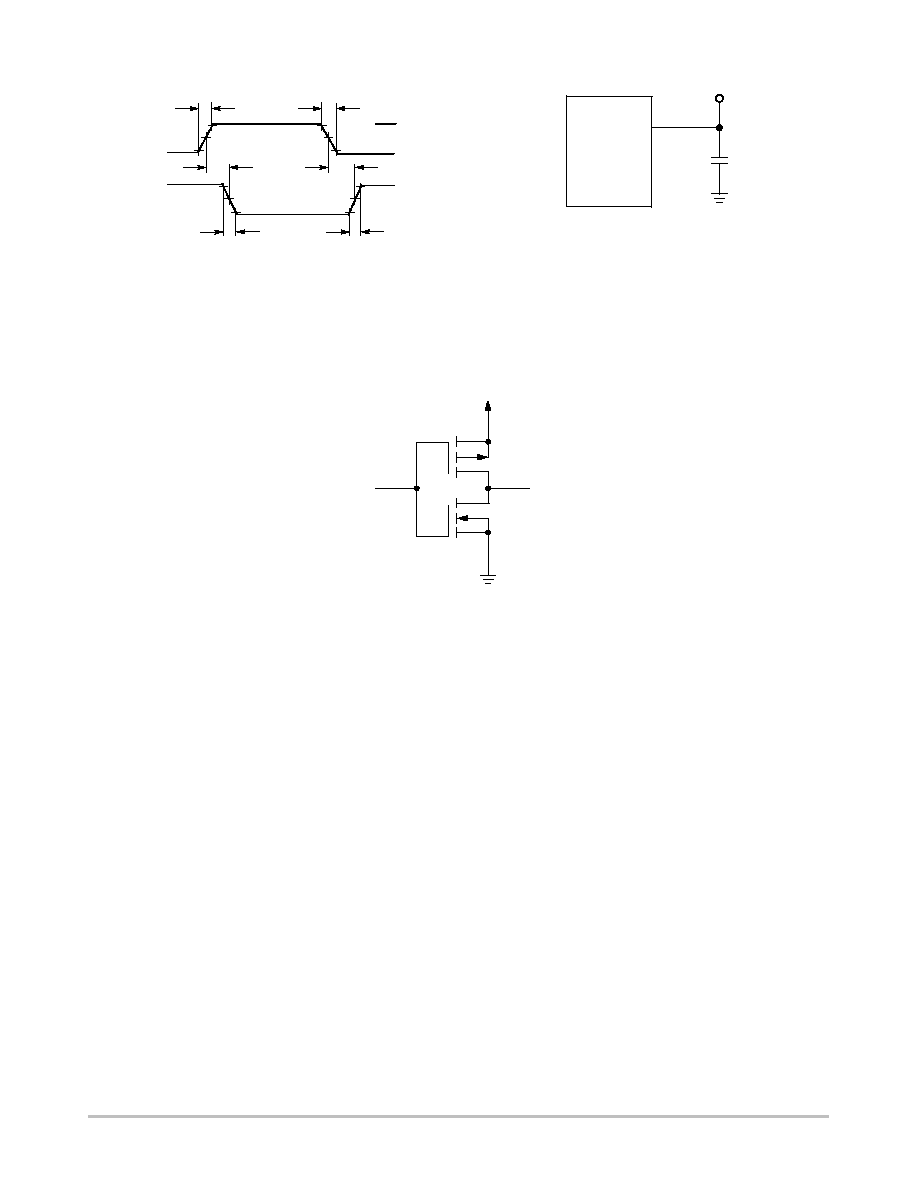
Figure 1. Switching Waveforms
tr
VCC
GND
90%
50%
10%
90%
50%
10%
INPUT A
OUTPUT Y
tPHL
tPLH
tTHL
tTLH
*Includes all probe and jig capacitance
Figure 2. Test Circuit
CL*
TEST POINT
DEVICE
UNDER
TEST
OUTPUT
LOGIC DETAIL
(1/6 of Device Shown)
tf
A
VCC
Y
MC74HCU04A
http://onsemi.com
5
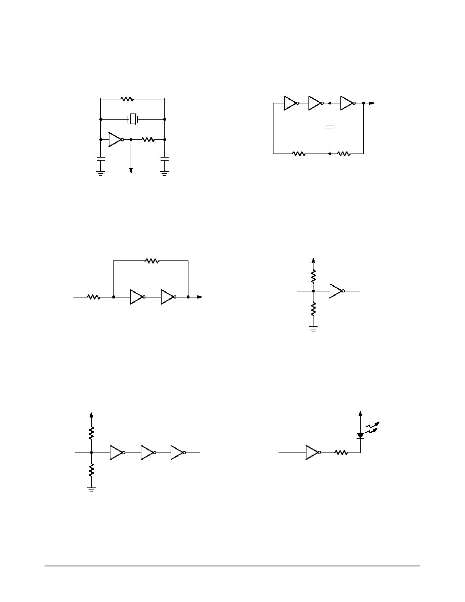
Crystal Oscillator
Stable RC Oscillator
Schmitt Trigger
High Input Impedance SingleStage Amplifier
with a 2 to 6 V Supply Range
MultiStage Amplifier
LED Driver
For reduced power supply current, use highefficiency LEDs
such as the HewlettPackard HLMP series or equivalent.
R2
1/6 HCU04A
C1
R2 > > R1
C1 < C2
Vout
C2
R1
R2
R1
C
1/6 HCU04A
1/6 HCU04A
1/6 HCU04A
Vout
R2
R1
Vin
Vout
1/6 HCU04A
1/6 HCU04A
R2 > 6R1
VCC
INPUT
OUTPUT
1 M
1 M
1/6 HCU04A
VCC
INPUT
OUTPUT
1/6 HCU04A
1/6 HCU04A
1/6 HCU04A
+ V
1/6 HCU04A
TYPICAL APPLICATIONS
MC74HCU04A
http://onsemi.com
6
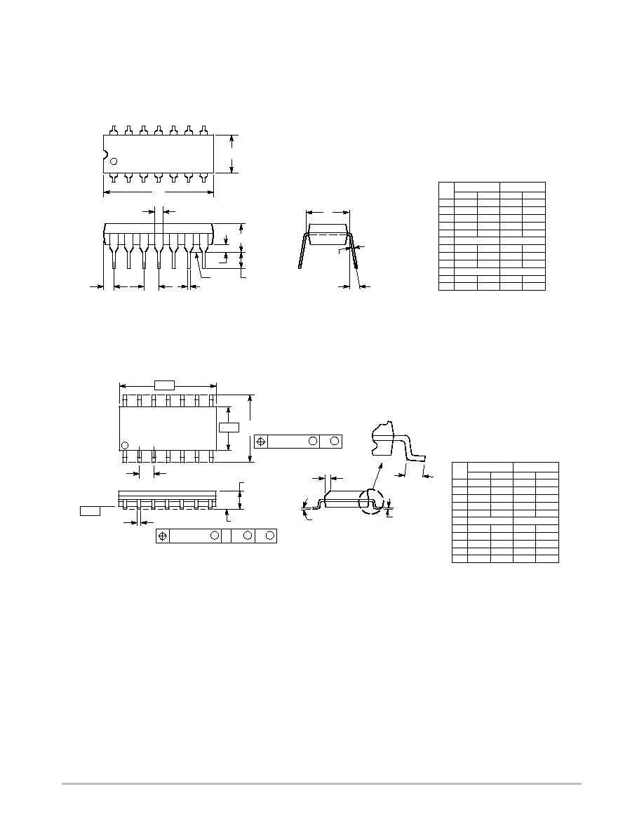
PACKAGE DIMENSIONS
PDIP14
N SUFFIX
CASE 64606
ISSUE L
NOTES:
1. LEADS WITHIN 0.13 (0.005) RADIUS OF TRUE
POSITION AT SEATING PLANE AT MAXIMUM
MATERIAL CONDITION.
2. DIMENSION L TO CENTER OF LEADS WHEN
FORMED PARALLEL.
3. DIMENSION B DOES NOT INCLUDE MOLD
FLASH.
4. ROUNDED CORNERS OPTIONAL.
1
7
14
8
B
A
F
H
G
D
K
C
N
L
J
M
SEATING
PLANE
DIM
MIN
MAX
MIN
MAX
MILLIMETERS
INCHES
A
0.715
0.770
18.16
19.56
B
0.240
0.260
6.10
6.60
C
0.145
0.185
3.69
4.69
D
0.015
0.021
0.38
0.53
F
0.040
0.070
1.02
1.78
G
0.100 BSC
2.54 BSC
H
0.052
0.095
1.32
2.41
J
0.008
0.015
0.20
0.38
K
0.115
0.135
2.92
3.43
L
0.300 BSC
7.62 BSC
M
0
10 0 10
N
0.015
0.039
0.39
1.01
_
_
_
_
SOIC14
D SUFFIX
CASE 751A03
ISSUE F
NOTES:
1. DIMENSIONING AND TOLERANCING PER ANSI
Y14.5M, 1982.
2. CONTROLLING DIMENSION: MILLIMETER.
3. DIMENSIONS A AND B DO NOT INCLUDE
MOLD PROTRUSION.
4. MAXIMUM MOLD PROTRUSION 0.15 (0.006)
PER SIDE.
5. DIMENSION D DOES NOT INCLUDE DAMBAR
PROTRUSION. ALLOWABLE DAMBAR
PROTRUSION SHALL BE 0.127 (0.005) TOTAL
IN EXCESS OF THE D DIMENSION AT
MAXIMUM MATERIAL CONDITION.
A
B
G
P
7 PL
14
8
7
1
M
0.25 (0.010)
B
M
S
B
M
0.25 (0.010)
A
S
T
T
F
R
X 45
SEATING
PLANE
D
14 PL
K
C
J
M
_
DIM
MIN
MAX
MIN
MAX
INCHES
MILLIMETERS
A
8.55
8.75
0.337
0.344
B
3.80
4.00
0.150
0.157
C
1.35
1.75
0.054
0.068
D
0.35
0.49
0.014
0.019
F
0.40
1.25
0.016
0.049
G
1.27 BSC
0.050 BSC
J
0.19
0.25
0.008
0.009
K
0.10
0.25
0.004
0.009
M
0
7
0
7
P
5.80
6.20
0.228
0.244
R
0.25
0.50
0.010
0.019
_
_
_
_
MC74HCU04A
http://onsemi.com
7
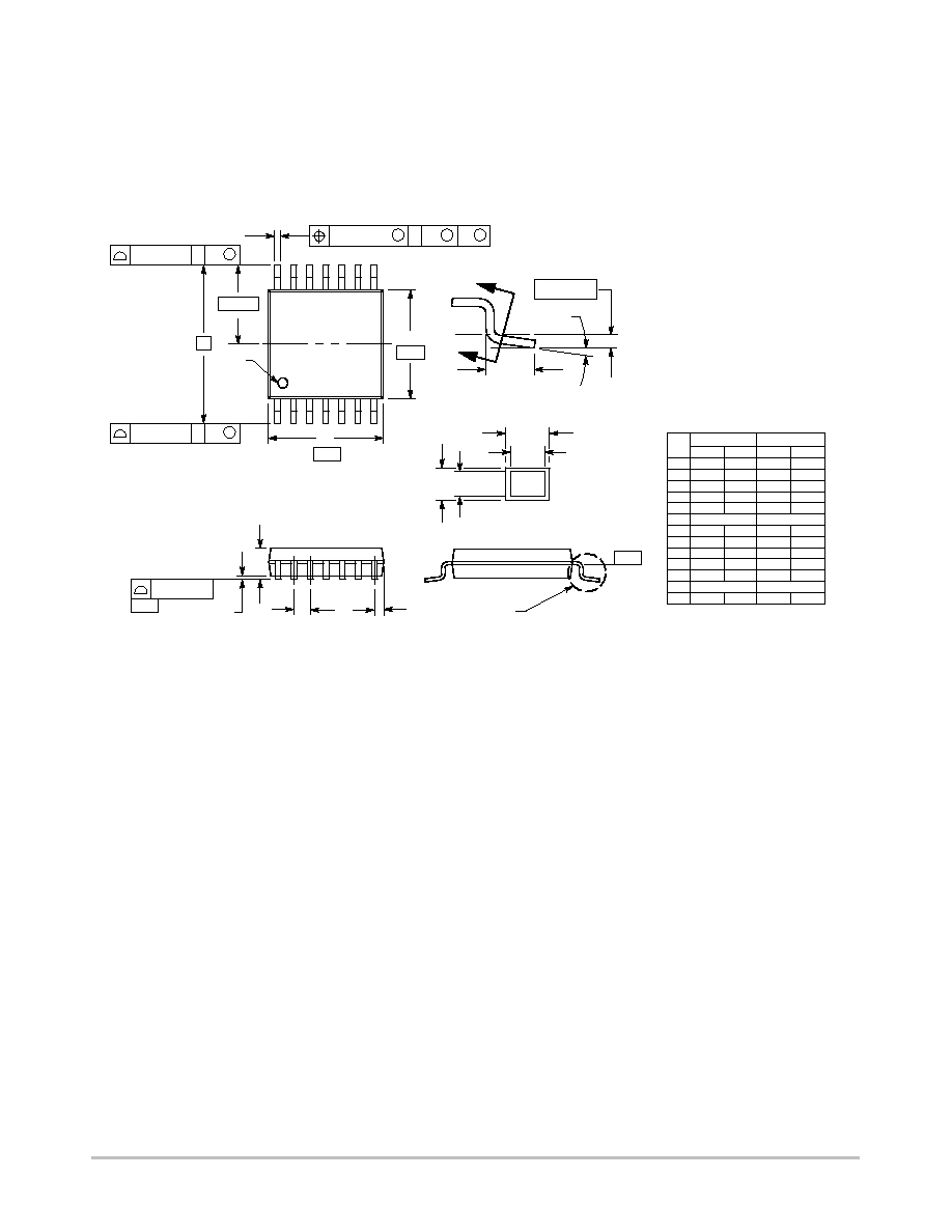
PACKAGE DIMENSIONS
TSSOP14
DT SUFFIX
CASE 948G01
ISSUE O
DIM
MIN
MAX
MIN
MAX
INCHES
MILLIMETERS
A
4.90
5.10
0.193
0.200
B
4.30
4.50
0.169
0.177
C
1.20
0.047
D
0.05
0.15
0.002
0.006
F
0.50
0.75
0.020
0.030
G
0.65 BSC
0.026 BSC
H
0.50
0.60
0.020
0.024
J
0.09
0.20
0.004
0.008
J1
0.09
0.16
0.004
0.006
K
0.19
0.30
0.007
0.012
K1
0.19
0.25
0.007
0.010
L
6.40 BSC
0.252 BSC
M
0
8
0
8
NOTES:
1. DIMENSIONING AND TOLERANCING PER ANSI
Y14.5M, 1982.
2. CONTROLLING DIMENSION: MILLIMETER.
3. DIMENSION A DOES NOT INCLUDE MOLD FLASH,
PROTRUSIONS OR GATE BURRS. MOLD FLASH
OR GATE BURRS SHALL NOT EXCEED 0.15
(0.006) PER SIDE.
4. DIMENSION B DOES NOT INCLUDE INTERLEAD
FLASH OR PROTRUSION. INTERLEAD FLASH OR
PROTRUSION SHALL NOT EXCEED
0.25 (0.010) PER SIDE.
5. DIMENSION K DOES NOT INCLUDE DAMBAR
PROTRUSION. ALLOWABLE DAMBAR
PROTRUSION SHALL BE 0.08 (0.003) TOTAL IN
EXCESS OF THE K DIMENSION AT MAXIMUM
MATERIAL CONDITION.
6. TERMINAL NUMBERS ARE SHOWN FOR
REFERENCE ONLY.
7. DIMENSION A AND B ARE TO BE DETERMINED
AT DATUM PLANE W.
_
_
_
_
S
U
0.15 (0.006) T
2X
L/2
S
U
M
0.10 (0.004)
V
S
T
L
U
SEATING
PLANE
0.10 (0.004)
T
ÇÇ
ÇÇ
SECTION NN
DETAIL E
J J1
K
K1
ÉÉ
ÉÉ
DETAIL E
F
M
W
0.25 (0.010)
8
14
7
1
PIN 1
IDENT.
H
G
A
D
C
B
S
U
0.15 (0.006) T
V
14X REF
K
N
N
MC74HCU04A
http://onsemi.com
8
ON Semiconductor and are trademarks of Semiconductor Components Industries, LLC (SCILLC). SCILLC reserves the right to make changes
without further notice to any products herein. SCILLC makes no warranty, representation or guarantee regarding the suitability of its products for any particular
purpose, nor does SCILLC assume any liability arising out of the application or use of any product or circuit, and specifically disclaims any and all liability,
including without limitation special, consequential or incidental damages. "Typical" parameters which may be provided in SCILLC data sheets and/or
specifications can and do vary in different applications and actual performance may vary over time. All operating parameters, including "Typicals" must be
validated for each customer application by customer's technical experts. SCILLC does not convey any license under its patent rights nor the rights of others.
SCILLC products are not designed, intended, or authorized for use as components in systems intended for surgical implant into the body, or other applications
intended to support or sustain life, or for any other application in which the failure of the SCILLC product could create a situation where personal injury or
death may occur. Should Buyer purchase or use SCILLC products for any such unintended or unauthorized application, Buyer shall indemnify and hold
SCILLC and its officers, employees, subsidiaries, affiliates, and distributors harmless against all claims, costs, damages, and expenses, and reasonable
attorney fees arising out of, directly or indirectly, any claim of personal injury or death associated with such unintended or unauthorized use, even if such claim
alleges that SCILLC was negligent regarding the design or manufacture of the part. SCILLC is an Equal Opportunity/Affirmative Action Employer.
PUBLICATION ORDERING INFORMATION
CENTRAL/SOUTH AMERICA:
Spanish Phone: 3033087143 (MonFri 8:00am to 5:00pm MST)
Email: ONlitspanish@hibbertco.com
ASIA/PACIFIC: LDC for ON Semiconductor Asia Support
Phone: 3036752121 (TueFri 9:00am to 1:00pm, Hong Kong Time)
Toll Free from Hong Kong & Singapore:
00180044223781
Email: ONlitasia@hibbertco.com
JAPAN: ON Semiconductor, Japan Customer Focus Center
4321 NishiGotanda, Shinagawaku, Tokyo, Japan 1418549
Phone: 81357402745
Email: r14525@onsemi.com
ON Semiconductor Website: http://onsemi.com
For additional information, please contact your local
Sales Representative.
MC74HCU04A/D
NORTH AMERICA Literature Fulfillment:
Literature Distribution Center for ON Semiconductor
P.O. Box 5163, Denver, Colorado 80217 USA
Phone: 3036752175 or 8003443860 Toll Free USA/Canada
Fax: 3036752176 or 8003443867 Toll Free USA/Canada
Email: ONlit@hibbertco.com
Fax Response Line: 3036752167 or 8003443810 Toll Free USA/Canada
N. American Technical Support: 8002829855 Toll Free USA/Canada
EUROPE: LDC for ON Semiconductor European Support
German Phone: (+1) 3033087140 (MF 1:00pm to 5:00pm Munich Time)
Email: ONlitgerman@hibbertco.com
French Phone: (+1) 3033087141 (MF 1:00pm to 5:00pm Toulouse Time)
Email: ONlitfrench@hibbertco.com
English Phone: (+1) 3033087142 (MF 12:00pm to 5:00pm UK Time)
Email: ONlit@hibbertco.com
EUROPEAN TOLLFREE ACCESS*: 0080044223781
*Available from Germany, France, Italy, England, Ireland