©
Semiconductor Components Industries, LLC, 2005
July, 2005 - Rev. 11
1
Publication Order Number:
MC74HC245A/D
MC74HC245A
Octal 3-State Noninverting
Bus Transceiver
High-Performance Silicon-Gate CMOS
The MC74HC245A is identical in pinout to the LS245. The device
inputs are compatible with standard CMOS outputs; with pull-up
resistors, they are compatible with LSTTL outputs.
The HC245A is a 3-state noninverting transceiver that is used for
2-way asynchronous communication between data buses. The device
has an active-low Output Enable pin, which is used to place the I/O
ports into high-impedance states. The Direction control determines
whether data flows from A to B or from B to A.
Features
·
Output Drive Capability: 15 LSTTL Loads
·
Outputs Directly Interface to CMOS, NMOS, and TTL
·
Operating Voltage Range: 2.0 to 6.0 V
·
Low Input Current: 1
mA
·
High Noise Immunity Characteristic of CMOS Devices
·
In Compliance with the Requirements Defined by JEDEC Standard
No. 7A
·
Moisture Sensitivity: MSL1 for All Packages
·
Chip Complexity: 308 FETs or 77 Equivalent Gates
·
Pb-Free Packages are Available*
*For additional information on our Pb-Free strategy and soldering details, please
download the ON Semiconductor Soldering and Mounting Techniques
Reference Manual, SOLDERRM/D.
http://onsemi.com
20
1
1
20
MARKING
DIAGRAMS
SOIC-20
DW SUFFIX
CASE 751D
74HC245A
AWLYYWWG
HC
245A
ALYW
G
G
TSSOP-20
DT SUFFIX
CASE 948E
SOEIAJ-20
F SUFFIX
CASE 967
74HC245A
AWLYWWG
1
1
1
20
1
20
20
20
See detailed ordering and shipping information in the package
dimensions section on page 2 of this data sheet.
ORDERING INFORMATION
PDIP-20
N SUFFIX
CASE 738
1
20
MC74HC245AN
AWLYYWWG
1
20
A
= Assembly Location
WL, L
= Wafer Lot
YY, Y
= Year
WW, W
= Work Week
G
= Pb-Free Package
G
= Pb-Free Package
(Note: Microdot may be in either location)
MC74HC245A
http://onsemi.com
2
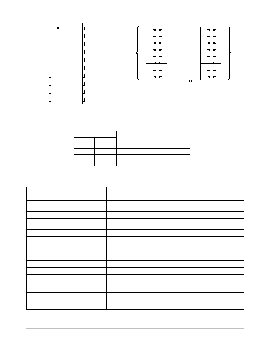
Figure 1. Pin Assignment
A5
A3
A2
A1
DIRECTION
GND
A8
A7
A6
A4
5
4
3
2
1
10
9
8
7
6
14
15
16
17
18
19
20
11
12
13
B3
B2
B1
OUTPUT ENABLE
V
CC
B8
B7
B6
B5
B4
A
DATA
PORT
A8
A7
A6
A5
A3
A4
A2
A1
9
8
7
6
5
4
3
2
DIRECTION
OUTPUT ENABLE
1
19
PIN 10 = GND
PIN 20 = V
CC
18
17
16
15
14
13
12
11
B1
B2
B3
B4
B5
B6
B7
B8
B
DATA
PORT
Figure 2. Logic Diagram
FUNCTION TABLE
Control Inputs
Operation
Output
Enable
Direction
L
L
Data Transmitted from Bus B to Bus A
L
H
Data Transmitted from Bus A to Bus B
H
X
Buses Isolated (High-Impedance State)
X = don't care
ORDERING INFORMATION
Device
Package
Shipping
MC74HC245AN
PDIP-20
18 Units / Rail
MC74HC245ANG
PDIP-20
(Pb-Free)
18 Units / Rail
MC74HC245ADW
SOIC-20 WIDE
38 Units / Rail
MC74HC245ADWG
SOIC-20 WIDE
(Pb-Free)
38 Units / Rail
MC74HC245ADWR2
SOIC-20 WIDE
1000 Tape & Reel
MC74HC245ADWR2G
SOIC-20 WIDE
(Pb-Free)
1000 Tape & Reel
MC74HC245ADT
TSSOP-20*
75 Units / Rail
MC74HC245ADTG
TSSOP-20*
75 Units / Rail
MC74HC245ADTR2
TSSOP-20*
2500 Tape & Reel
MC74HC245ADTR2G
TSSOP-20*
2500 Tape & Reel
MC74HC245AF
SOEIAJ-20
40 Units / Rail
MC74HC245AFG
SOEIAJ-20
(Pb-Free)
40 Units / Rail
MC74HC245AFEL
SOEIAJ-20
2000 Tape & Reel
MC74HC245AFELG
SOEIAJ-20
(Pb-Free)
2000 Tape & Reel
For information on tape and reel specifications, including part orientation and tape sizes, please refer to our Tape and Reel Packaging
Specifications Brochure, BRD8011/D.
*This package is inherently Pb-Free.

MC74HC245A
http://onsemi.com
3
MAXIMUM RATINGS
(Note 1)
Symbol
Parameter
Value
Unit
V
CC
DC Supply Voltage
*
0.5 to
)
7.0
V
V
IN
DC Input Voltage
*
0.5 to V
CC
)
0.5
V
V
OUT
DC Output Voltage
(Note 2)
*
0.5 to V
CC
)
0.5
V
I
IK
DC Input Diode Current
$
20
mA
I
OK
DC Output Diode Current
$
35
mA
I
OUT
DC Output Sink Current
$
35
mA
I
CC
DC Supply Current per Supply Pin
$
75
mA
I
GND
DC Ground Current per Ground Pin
$
75
mA
T
STG
Storage Temperature Range
*
65 to
)
150
_
C
T
L
Lead Temperature, 1 mm from Case for 10 Seconds
260
_
C
T
J
Junction Temperature Under Bias
)
150
_
C
q
JA
Thermal Resistance
PDIP
SOIC
TSSOP
67
96
128
_
C/W
P
D
Power Dissipation in Still Air at 85
_
C
PDIP
SOIC
TSSOP
750
500
450
mW
MSL
Moisture Sensitivity
Level 1
F
R
Flammability Rating
Oxygen Index: 30% to 35%
UL 94 V-0 @ 0.125 in
V
ESD
ESD Withstand Voltage
Human Body Model (Note 3)
Machine Model (Note 4)
Charged Device Model (Note 5)
u
2000
u
200
u
1000
V
I
LATCHUP
Latchup Performance
Above V
CC
and Below GND at 85
_
C (Note 6)
$
300
mA
Maximum ratings are those values beyond which device damage can occur. Maximum ratings applied to the device are individual stress limit
values (not normal operating conditions) and are not valid simultaneously. If these limits are exceeded, device functional operation is not implied,
damage may occur and reliability may be affected.
1. Measured with minimum pad spacing on an FR4 board, using 10 mm-by-1 inch, 20 ounce copper trace with no air flow.
2. I
O
absolute maximum rating must observed.
3. Tested to EIA/JESD22-A114-A.
4. Tested to EIA/JESD22-A115-A.
5. Tested to JESD22-C101-A.
6. Tested to EIA/JESD78.
RECOMMENDED OPERATING CONDITIONS
ÎÎÎÎ
ÎÎÎÎ
Symbol
ÎÎÎÎÎÎÎÎÎÎÎÎÎÎÎÎÎÎÎÎÎ
ÎÎÎÎÎÎÎÎÎÎÎÎÎÎÎÎÎÎÎÎÎ
Parameter
ÎÎÎÎÎ
ÎÎÎÎÎ
Min
ÎÎÎÎ
ÎÎÎÎ
Max
ÎÎÎ
ÎÎÎ
Unit
ÎÎÎÎ
ÎÎÎÎ
V
CC
ÎÎÎÎÎÎÎÎÎÎÎÎÎÎÎÎÎÎÎÎÎ
ÎÎÎÎÎÎÎÎÎÎÎÎÎÎÎÎÎÎÎÎÎ
DC Supply Voltage (Referenced to GND)
ÎÎÎÎÎ
ÎÎÎÎÎ
2.0
ÎÎÎÎ
ÎÎÎÎ
6.0
ÎÎÎ
ÎÎÎ
V
ÎÎÎÎ
ÎÎÎÎ
V
in
, V
out
ÎÎÎÎÎÎÎÎÎÎÎÎÎÎÎÎÎÎÎÎÎ
ÎÎÎÎÎÎÎÎÎÎÎÎÎÎÎÎÎÎÎÎÎ
DC Input Voltage, Output Voltage (Referenced to GND)
ÎÎÎÎÎ
ÎÎÎÎÎ
0
ÎÎÎÎ
ÎÎÎÎ
V
CC
ÎÎÎ
ÎÎÎ
V
ÎÎÎÎ
ÎÎÎÎ
T
A
ÎÎÎÎÎÎÎÎÎÎÎÎÎÎÎÎÎÎÎÎÎ
ÎÎÎÎÎÎÎÎÎÎÎÎÎÎÎÎÎÎÎÎÎ
Operating Temperature, All Package Types
ÎÎÎÎÎ
ÎÎÎÎÎ
55
ÎÎÎÎ
ÎÎÎÎ
+125
ÎÎÎ
ÎÎÎ
_
C
ÎÎÎÎ
ÎÎÎÎ
ÎÎÎÎ
t
r
, t
f
ÎÎÎÎÎÎÎÎÎÎÎÎÎÎÎÎÎÎÎÎÎ
ÎÎÎÎÎÎÎÎÎÎÎÎÎÎÎÎÎÎÎÎÎ
ÎÎÎÎÎÎÎÎÎÎÎÎÎÎÎÎÎÎÎÎÎ
Input Rise and Fall Time
V
CC
= 2.0 V
(Figure 3)
V
CC
= 4.5 V
V
CC
= 6.0 V
ÎÎÎÎÎ
ÎÎÎÎÎ
ÎÎÎÎÎ
0
0
0
ÎÎÎÎ
ÎÎÎÎ
ÎÎÎÎ
1000
500
400
ÎÎÎ
ÎÎÎ
ÎÎÎ
ns
MC74HC245A
http://onsemi.com
4
DC ELECTRICAL CHARACTERISTICS
(Voltages Referenced to GND)
ÎÎÎÎ
ÎÎÎÎ
ÎÎÎÎÎÎÎÎÎÎ
ÎÎÎÎÎÎÎÎÎÎ
ÎÎÎÎÎÎÎÎÎ
ÎÎÎÎÎÎÎÎÎ
ÎÎÎ
ÎÎÎ
ÎÎÎÎÎÎÎÎÎÎ
ÎÎÎÎÎÎÎÎÎÎ
Guaranteed Limit
ÎÎ
ÎÎ
ÎÎÎÎ
ÎÎÎÎ
Symbol
ÎÎÎÎÎÎÎÎÎÎ
ÎÎÎÎÎÎÎÎÎÎ
Parameter
ÎÎÎÎÎÎÎÎÎ
ÎÎÎÎÎÎÎÎÎ
Test Conditions
ÎÎÎ
ÎÎÎ
V
CC
V
ÎÎÎÎ
ÎÎÎÎ
55 to
25
_
C
ÎÎÎÎ
ÎÎÎÎ
v
85
_
C
ÎÎÎÎ
ÎÎÎÎ
v
125
_
C
ÎÎ
ÎÎ
Unit
ÎÎÎÎ
ÎÎÎÎ
ÎÎÎÎ
ÎÎÎÎ
V
IH
ÎÎÎÎÎÎÎÎÎÎ
ÎÎÎÎÎÎÎÎÎÎ
Î ÎÎÎÎÎÎÎÎÎ
ÎÎÎÎÎÎÎÎÎÎ
Minimum High-Level Input Voltage
ÎÎÎÎÎÎÎÎÎ
ÎÎÎÎÎÎÎÎÎ
Î ÎÎÎÎÎÎÎÎ
ÎÎÎÎÎÎÎÎÎ
V
out
= V
CC
0.1 V
|I
out
|
v
20
m
A
ÎÎÎ
ÎÎÎ
ÎÎÎ
ÎÎÎ
2.0
3.0
4.5
6.0
ÎÎÎÎ
ÎÎÎÎ
ÎÎÎÎ
ÎÎÎÎ
1.5
2.1
3.15
4.2
ÎÎÎÎ
ÎÎÎÎ
ÎÎÎÎ
ÎÎÎÎ
1.5
2.1
3.15
4.2
ÎÎÎÎ
ÎÎÎÎ
ÎÎÎÎ
ÎÎÎÎ
1.5
2.1
3.15
4.2
ÎÎ
ÎÎ
ÎÎ
ÎÎ
V
ÎÎÎÎ
ÎÎÎÎ
ÎÎÎÎ
ÎÎÎÎ
V
IL
ÎÎÎÎÎÎÎÎÎÎ
ÎÎÎÎÎÎÎÎÎÎ
Î ÎÎÎÎÎÎÎÎÎ
ÎÎÎÎÎÎÎÎÎÎ
Maximum Low-Level Input Voltage
ÎÎÎÎÎÎÎÎÎ
ÎÎÎÎÎÎÎÎÎ
Î ÎÎÎÎÎÎÎÎ
ÎÎÎÎÎÎÎÎÎ
V
out
= 0.1 V
|I
out
|
v
20
m
A
ÎÎÎ
ÎÎÎ
ÎÎÎ
ÎÎÎ
2.0
3.0
4.5
6.0
ÎÎÎÎ
ÎÎÎÎ
ÎÎÎÎ
ÎÎÎÎ
0.5
0.9
1.35
1.8
ÎÎÎÎ
ÎÎÎÎ
ÎÎÎÎ
ÎÎÎÎ
0.5
0.9
1.35
1.8
ÎÎÎÎ
ÎÎÎÎ
ÎÎÎÎ
ÎÎÎÎ
0.5
0.9
1.35
1.8
ÎÎ
ÎÎ
ÎÎ
ÎÎ
V
ÎÎÎÎ
ÎÎÎÎ
ÎÎÎÎ
ÎÎÎÎ
ÎÎÎÎ
V
OH
ÎÎÎÎÎÎÎÎÎÎ
ÎÎÎÎÎÎÎÎÎÎ
Î ÎÎÎÎÎÎÎÎÎ
Î ÎÎÎÎÎÎÎÎÎ
ÎÎÎÎÎÎÎÎÎÎ
Minimum High-Level Output
Voltage
ÎÎÎÎÎÎÎÎÎ
ÎÎÎÎÎÎÎÎÎ
ÎÎÎÎÎÎÎÎÎ
V
in
= V
IH
|I
out
|
v
20
m
A
ÎÎÎ
ÎÎÎ
ÎÎÎ
2.0
4.5
6.0
ÎÎÎÎ
ÎÎÎÎ
ÎÎÎÎ
1.9
4.4
5.9
ÎÎÎÎ
ÎÎÎÎ
ÎÎÎÎ
1.9
4.4
5.9
ÎÎÎÎ
ÎÎÎÎ
ÎÎÎÎ
1.9
4.4
5.9
ÎÎ
ÎÎ
ÎÎ
ÎÎ
ÎÎ
V
ÎÎÎÎÎÎÎÎÎ
ÎÎÎÎÎÎÎÎÎ
ÎÎÎÎÎÎÎÎÎ
V
in
= V
IH
|I
out
|
v
2.4 mA
|I
out
|
v
6.0 mA
|I
out
|
v
7.8 mA
ÎÎÎ
ÎÎÎ
ÎÎÎ
3.0
4.5
6.0
ÎÎÎÎ
ÎÎÎÎ
ÎÎÎÎ
2.48
3.98
5.48
ÎÎÎÎ
ÎÎÎÎ
ÎÎÎÎ
2.34
3.84
5.34
ÎÎÎÎ
ÎÎÎÎ
ÎÎÎÎ
2.2
3.7
5.2
ÎÎÎÎ
ÎÎÎÎ
ÎÎÎÎ
ÎÎÎÎ
ÎÎÎÎ
V
OL
ÎÎÎÎÎÎÎÎÎÎ
ÎÎÎÎÎÎÎÎÎÎ
Î ÎÎÎÎÎÎÎÎÎ
Î ÎÎÎÎÎÎÎÎÎ
ÎÎÎÎÎÎÎÎÎÎ
Maximum Low-Level Output
Voltage
ÎÎÎÎÎÎÎÎÎ
ÎÎÎÎÎÎÎÎÎ
ÎÎÎÎÎÎÎÎÎ
V
in
= V
IL
|I
out
|
v
20
m
A
ÎÎÎ
ÎÎÎ
ÎÎÎ
2.0
4.5
6.0
ÎÎÎÎ
ÎÎÎÎ
ÎÎÎÎ
0.1
0.1
0.1
ÎÎÎÎ
ÎÎÎÎ
ÎÎÎÎ
0.1
0.1
0.1
ÎÎÎÎ
ÎÎÎÎ
ÎÎÎÎ
0.1
0.1
0.1
ÎÎ
ÎÎ
ÎÎ
ÎÎ
ÎÎ
V
ÎÎÎÎÎÎÎÎÎ
ÎÎÎÎÎÎÎÎÎ
ÎÎÎÎÎÎÎÎÎ
V
in
= V
IL
|I
out
|
v
2.4 mA
|I
out
|
v
6.0 mA
|I
out
|
v
7.8 mA
ÎÎÎ
ÎÎÎ
ÎÎÎ
3.0
4.5
6.0
ÎÎÎÎ
ÎÎÎÎ
ÎÎÎÎ
0.26
0.26
0.26
ÎÎÎÎ
ÎÎÎÎ
ÎÎÎÎ
0.33
0.33
0.33
ÎÎÎÎ
ÎÎÎÎ
ÎÎÎÎ
0.4
0.4
0.4
ÎÎÎÎ
ÎÎÎÎ
I
in
ÎÎÎÎÎÎÎÎÎÎ
ÎÎÎÎÎÎÎÎÎÎ
Maximum Input Leakage Current
ÎÎÎÎÎÎÎÎÎ
ÎÎÎÎÎÎÎÎÎ
V
in
= V
CC
or GND
ÎÎÎ
ÎÎÎ
6.0
ÎÎÎÎ
ÎÎÎÎ
±
0.1
ÎÎÎÎ
ÎÎÎÎ
±
1.0
ÎÎÎÎ
ÎÎÎÎ
±
1.0
ÎÎ
ÎÎ
m
A
ÎÎÎÎ
ÎÎÎÎ
ÎÎÎÎ
I
OZ
ÎÎÎÎÎÎÎÎÎÎ
ÎÎÎÎÎÎÎÎÎÎ
ÎÎÎÎÎÎÎÎÎÎ
Maximum Three-State Leakage
Current
ÎÎÎÎÎÎÎÎÎ
ÎÎÎÎÎÎÎÎÎ
ÎÎÎÎÎÎÎÎÎ
Output in High-Impedance State
V
in
= V
IL
or V
IH
V
out
= V
CC
or GND
ÎÎÎ
ÎÎÎ
ÎÎÎ
6.0
ÎÎÎÎ
ÎÎÎÎ
ÎÎÎÎ
±
0.5
ÎÎÎÎ
ÎÎÎÎ
ÎÎÎÎ
±
5.0
ÎÎÎÎ
ÎÎÎÎ
ÎÎÎÎ
±
10
ÎÎ
ÎÎ
ÎÎ
m
A
ÎÎÎÎ
ÎÎÎÎ
ÎÎÎÎ
I
CC
ÎÎÎÎÎÎÎÎÎÎ
ÎÎÎÎÎÎÎÎÎÎ
ÎÎÎÎÎÎÎÎÎÎ
Maximum Quiescent Supply
Current (per Package)
ÎÎÎÎÎÎÎÎÎ
ÎÎÎÎÎÎÎÎÎ
ÎÎÎÎÎÎÎÎÎ
V
in
= V
CC
or GND
I
out
= 0
m
A
ÎÎÎ
ÎÎÎ
ÎÎÎ
6.0
ÎÎÎÎ
ÎÎÎÎ
ÎÎÎÎ
4.0
ÎÎÎÎ
ÎÎÎÎ
ÎÎÎÎ
40
ÎÎÎÎ
ÎÎÎÎ
ÎÎÎÎ
160
ÎÎ
ÎÎ
ÎÎ
m
A
7. Information on typical parametric values and high frequency or heavy load considerations can be found in the ON Semiconductor
High-Speed CMOS Data Book (DL129/D).
AC ELECTRICAL CHARACTERISTICS
(C
L
= 50 pF, Input t
r
= t
f
= 6 ns)
ÎÎÎÎ
ÎÎÎÎ
ÎÎÎÎ
Symbol
ÎÎÎÎÎÎÎÎÎÎÎÎÎÎÎÎÎÎ
ÎÎÎÎÎÎÎÎÎÎÎÎÎÎÎÎÎÎ
ÎÎÎÎÎÎÎÎÎÎÎÎÎÎÎÎÎÎ
Parameter
ÎÎÎ
ÎÎÎ
ÎÎÎ
V
CC
V
ÎÎÎÎÎÎÎÎÎÎ
ÎÎÎÎÎÎÎÎÎÎ
Guaranteed Limit
ÎÎ
ÎÎ
ÎÎ
Unit
ÎÎÎÎ
ÎÎÎÎ
55 to
25
_
C
ÎÎÎÎ
ÎÎÎÎ
v
85
_
C
ÎÎÎÎ
ÎÎÎÎ
v
125
_
C
ÎÎÎÎ
ÎÎÎÎ
ÎÎÎÎ
ÎÎÎÎ
t
PLH
,
t
PHL
ÎÎÎÎÎÎÎÎÎÎÎÎÎÎÎÎÎÎ
ÎÎÎÎÎÎÎÎÎÎÎÎÎÎÎÎÎÎ
Î ÎÎÎÎÎÎÎÎÎÎÎÎÎÎÎÎÎ
ÎÎÎÎÎÎÎÎÎÎÎÎÎÎÎÎÎÎ
Maximum Propagation Delay,
A to B, B to A
(Figures 1 and 3)
ÎÎÎ
ÎÎÎ
ÎÎÎ
ÎÎÎ
2.0
3.0
4.5
6.0
ÎÎÎÎ
ÎÎÎÎ
ÎÎÎÎ
ÎÎÎÎ
75
55
15
13
ÎÎÎÎ
ÎÎÎÎ
ÎÎÎÎ
ÎÎÎÎ
95
70
19
16
ÎÎÎÎ
ÎÎÎÎ
ÎÎÎÎ
ÎÎÎÎ
110
80
22
19
ÎÎ
ÎÎ
ÎÎ
ÎÎ
ns
ÎÎÎÎ
ÎÎÎÎ
ÎÎÎÎ
ÎÎÎÎ
t
PLZ
,
t
PHZ
ÎÎÎÎÎÎÎÎÎÎÎÎÎÎÎÎÎÎ
ÎÎÎÎÎÎÎÎÎÎÎÎÎÎÎÎÎÎ
Î ÎÎÎÎÎÎÎÎÎÎÎÎÎÎÎÎÎ
ÎÎÎÎÎÎÎÎÎÎÎÎÎÎÎÎÎÎ
Maximum Propagation Delay,
Direction or Output Enable to A or B
(Figures 2 and 4)
ÎÎÎ
ÎÎÎ
ÎÎÎ
ÎÎÎ
2.0
3.0
4.5
6.0
ÎÎÎÎ
ÎÎÎÎ
ÎÎÎÎ
ÎÎÎÎ
110
90
22
19
ÎÎÎÎ
ÎÎÎÎ
ÎÎÎÎ
ÎÎÎÎ
140
110
28
24
ÎÎÎÎ
ÎÎÎÎ
ÎÎÎÎ
ÎÎÎÎ
165
130
33
28
ÎÎ
ÎÎ
ÎÎ
ÎÎ
ns
ÎÎÎÎ
ÎÎÎÎ
ÎÎÎÎ
ÎÎÎÎ
t
PZL
,
t
PZH
ÎÎÎÎÎÎÎÎÎÎÎÎÎÎÎÎÎÎ
ÎÎÎÎÎÎÎÎÎÎÎÎÎÎÎÎÎÎ
Î ÎÎÎÎÎÎÎÎÎÎÎÎÎÎÎÎÎ
ÎÎÎÎÎÎÎÎÎÎÎÎÎÎÎÎÎÎ
Maximum Propagation Delay,
Output Enable to A or B
(Figures 2 and 4)
ÎÎÎ
ÎÎÎ
ÎÎÎ
ÎÎÎ
2.0
3.0
4.5
6.0
ÎÎÎÎ
ÎÎÎÎ
ÎÎÎÎ
ÎÎÎÎ
110
90
22
19
ÎÎÎÎ
ÎÎÎÎ
ÎÎÎÎ
ÎÎÎÎ
140
110
28
24
ÎÎÎÎ
ÎÎÎÎ
ÎÎÎÎ
ÎÎÎÎ
165
130
33
28
ÎÎ
ÎÎ
ÎÎ
ÎÎ
ns
ÎÎÎÎ
ÎÎÎÎ
ÎÎÎÎ
t
TLH
,
t
THL
ÎÎÎÎÎÎÎÎÎÎÎÎÎÎÎÎÎÎ
ÎÎÎÎÎÎÎÎÎÎÎÎÎÎÎÎÎÎ
ÎÎÎÎÎÎÎÎÎÎÎÎÎÎÎÎÎÎ
Maximum Output Transition Time,
Any Output
(Figures 1 and 3)
ÎÎÎ
ÎÎÎ
ÎÎÎ
2.0
3.0
4.5
6.0
ÎÎÎÎ
ÎÎÎÎ
ÎÎÎÎ
60
23
12
10
ÎÎÎÎ
ÎÎÎÎ
ÎÎÎÎ
75
27
15
13
ÎÎÎÎ
ÎÎÎÎ
ÎÎÎÎ
90
32
18
15
ÎÎ
ÎÎ
ÎÎ
ns
ÎÎÎÎ
ÎÎÎÎ
C
in
ÎÎÎÎÎÎÎÎÎÎÎÎÎÎÎÎÎÎ
ÎÎÎÎÎÎÎÎÎÎÎÎÎÎÎÎÎÎ
Maximum Input Capacitance (Pin 1 or Pin 19)
ÎÎÎ
ÎÎÎ
-
ÎÎÎÎ
ÎÎÎÎ
10
ÎÎÎÎ
ÎÎÎÎ
10
ÎÎÎÎ
ÎÎÎÎ
10
ÎÎ
ÎÎ
pF
ÎÎÎÎ
ÎÎÎÎ
ÎÎÎÎ
C
out
ÎÎÎÎÎÎÎÎÎÎÎÎÎÎÎÎÎÎ
ÎÎÎÎÎÎÎÎÎÎÎÎÎÎÎÎÎÎ
ÎÎÎÎÎÎÎÎÎÎÎÎÎÎÎÎÎÎ
Maximum Three-State I/O Capacitance
(I/O in High-Impedance State)
ÎÎÎ
ÎÎÎ
ÎÎÎ
-
ÎÎÎÎ
ÎÎÎÎ
ÎÎÎÎ
15
ÎÎÎÎ
ÎÎÎÎ
ÎÎÎÎ
15
ÎÎÎÎ
ÎÎÎÎ
ÎÎÎÎ
15
ÎÎ
ÎÎ
ÎÎ
pF
8. For propagation delays with loads other than 50 pF, and information on typical parametric values, see the ON Semiconductor High-Speed
CMOS Data Book (DL129/D).
C
PD
Power Dissipation Capacitance (Per Transceiver Channel) (Note 9)
Typical @ 25
°
C, V
CC
= 5.0 V
pF
40
9. Used to determine the no-load dynamic power consumption: P
D
= C
PD
V
CC
2
f + I
CC
V
CC
. For load considerations, see the ON
Semiconductor High-Speed CMOS Data Book (DL129/D).
MC74HC245A
http://onsemi.com
5
V
CC
GND
t
f
t
r
INPUT
A OR B
OUTPUT
B OR A
10%
50%
90%
10%
50%
90%
t
TLH
t
PLH
t
PHL
t
THL
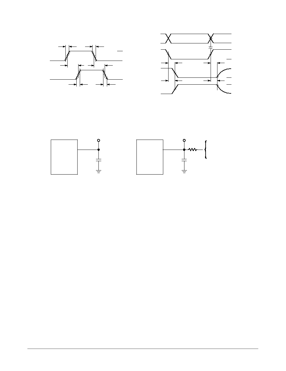
Figure 3. Switching Waveform
OUTPUT
ENABLE
A OR B
A OR B
50%
50%
50%
90%
10%
t
PZL
t
PLZ
t
PZH
t
PHZ
V
CC
GND
HIGH
IMPEDANCE
V
OL
V
OH
HIGH
IMPEDANCE
V
CC
GND
50%
Figure 4. Switching Waveform
DIRECTION
OUTPUT
*Includes all probe and jig capacitance
C
L
*
TEST POINT
DEVICE
UNDER
TEST
Figure 5. Test Circuit
*Includes all probe and jig capacitance
C
L
*
TEST POINT
DEVICE
UNDER
TEST
OUTPUT
Figure 6. Test Circuit
CONNECT TO V
CC
WHEN
TESTING t
PLZ
AND t
PZL
.
CONNECT TO GND WHEN
TESTING t
PHZ
AND t
PZH
.
1 k
W

MC74HC245A
http://onsemi.com
6
Figure 7. Expanded Logic Diagram
A
DATA
PORT
B
DATA
PORT
OUTPUT ENABLE
DIRECTION
A1
A2
A3
A4
A5
A6
A7
A8
2
3
4
5
6
7
8
9
19
1
B1
B2
B3
B4
B5
B6
B7
B8
18
17
16
15
14
13
12
11
MC74HC245A
http://onsemi.com
7
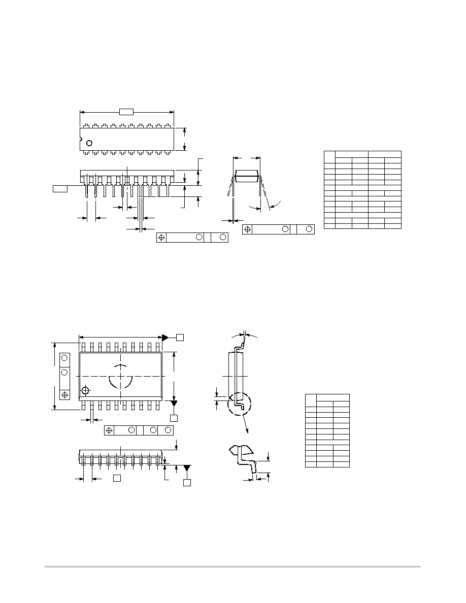
PACKAGE DIMENSIONS
PDIP-20
N SUFFIX
PLASTIC DIP PACKAGE
CASE 738-03
ISSUE E
NOTES:
1. DIMENSIONING AND TOLERANCING PER ANSI
Y14.5M, 1982.
2. CONTROLLING DIMENSION: INCH.
3. DIMENSION L TO CENTER OF LEAD WHEN
FORMED PARALLEL.
4. DIMENSION B DOES NOT INCLUDE MOLD
FLASH.
M
L
J
20 PL
M
B
M
0.25 (0.010)
T
DIM
MIN
MAX
MIN
MAX
MILLIMETERS
INCHES
A
25.66
27.17
1.010
1.070
B
6.10
6.60
0.240
0.260
C
3.81
4.57
0.150
0.180
D
0.39
0.55
0.015
0.022
G
2.54 BSC
0.100 BSC
J
0.21
0.38
0.008
0.015
K
2.80
3.55
0.110
0.140
L
7.62 BSC
0.300 BSC
M
0
15
0
15
N
0.51
1.01
0.020
0.040
_
_
_
_
E
1.27
1.77
0.050
0.070
1
11
10
20
-A-
SEATING
PLANE
K
N
F
G
D
20 PL
-T-
M
A
M
0.25 (0.010)
T
E
B
C
F
1.27 BSC
0.050 BSC
SOIC-20
DW SUFFIX
CASE 751D-05
ISSUE G
20
1
11
10
B
20X
H
10X
C
L
18X
A1
A
SEATING
PLANE
q
h
X 45
_
E
D
M
0.25
M
B
M
0.25
S
A
S
B
T
e
T
B
A
DIM
MIN
MAX
MILLIMETERS
A
2.35
2.65
A1
0.10
0.25
B
0.35
0.49
C
0.23
0.32
D
12.65
12.95
E
7.40
7.60
e
1.27 BSC
H
10.05
10.55
h
0.25
0.75
L
0.50
0.90
q
0
7
NOTES:
1. DIMENSIONS ARE IN MILLIMETERS.
2. INTERPRET DIMENSIONS AND TOLERANCES
PER ASME Y14.5M, 1994.
3. DIMENSIONS D AND E DO NOT INCLUDE MOLD
PROTRUSION.
4. MAXIMUM MOLD PROTRUSION 0.15 PER SIDE.
5. DIMENSION B DOES NOT INCLUDE DAMBAR
PROTRUSION. ALLOWABLE PROTRUSION
SHALL BE 0.13 TOTAL IN EXCESS OF B
DIMENSION AT MAXIMUM MATERIAL
CONDITION.
_
_

MC74HC245A
http://onsemi.com
8
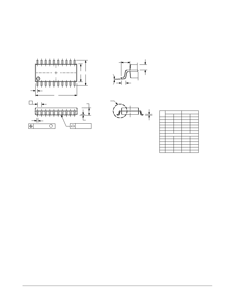
PACKAGE DIMENSIONS
TSSOP-20
DT SUFFIX
CASE 948E-02
ISSUE B
DIM
A
MIN
MAX
MIN
MAX
INCHES
6.60
0.260
MILLIMETERS
B
4.30
4.50
0.169
0.177
C
1.20
0.047
D
0.05
0.15
0.002
0.006
F
0.50
0.75
0.020
0.030
G
0.65 BSC
0.026 BSC
H
0.27
0.37
0.011
0.015
J
0.09
0.20
0.004
0.008
J1
0.09
0.16
0.004
0.006
K
0.19
0.30
0.007
0.012
K1
0.19
0.25
0.007
0.010
L
6.40 BSC
0.252 BSC
M
0 8 0 8
_
_
_
_
NOTES:
1. DIMENSIONING AND TOLERANCING
PER ANSI Y14.5M, 1982.
2. CONTROLLING DIMENSION:
MILLIMETER.
3. DIMENSION A DOES NOT INCLUDE
MOLD FLASH, PROTRUSIONS OR GATE
BURRS. MOLD FLASH OR GATE BURRS
SHALL NOT EXCEED 0.15 (0.006) PER
SIDE.
4. DIMENSION B DOES NOT INCLUDE
INTERLEAD FLASH OR PROTRUSION.
INTERLEAD FLASH OR PROTRUSION
SHALL NOT EXCEED 0.25 (0.010) PER
SIDE.
5. DIMENSION K DOES NOT INCLUDE
DAMBAR PROTRUSION. ALLOWABLE
DAMBAR PROTRUSION SHALL BE 0.08
(0.003) TOTAL IN EXCESS OF THE K
DIMENSION AT MAXIMUM MATERIAL
CONDITION.
6. TERMINAL NUMBERS ARE SHOWN
FOR REFERENCE ONLY.
7. DIMENSION A AND B ARE TO BE
DETERMINED AT DATUM PLANE -W-.
ÍÍÍÍ
ÍÍÍÍ
ÍÍÍÍ
1
10
11
20
PIN 1
IDENT
A
B
-T-
0.100 (0.004)
C
D
G
H
SECTION N-N
K
K1
J J1
N
N
M
F
-W-
SEATING
PLANE
-V-
-U-
S
U
M
0.10 (0.004)
V
S
T
20X REF
K
L
L/2
2X
S
U
0.15 (0.006) T
DETAIL E
0.25 (0.010)
DETAIL E
6.40
0.252
---
---
S
U
0.15 (0.006) T
MC74HC245A
http://onsemi.com
9
PACKAGE DIMENSIONS
SOEIAJ-20
F SUFFIX
CASE 967-01
ISSUE O
DIM
MIN
MAX
MIN
MAX
INCHES
---
2.05
---
0.081
MILLIMETERS
0.05
0.20
0.002
0.008
0.35
0.50
0.014
0.020
0.18
0.27
0.007
0.011
12.35
12.80
0.486
0.504
5.10
5.45
0.201
0.215
1.27 BSC
0.050 BSC
7.40
8.20
0.291
0.323
0.50
0.85
0.020
0.033
1.10
1.50
0.043
0.059
0
0.70
0.90
0.028
0.035
---
0.81
---
0.032
A
1
H
E
Q
1
L
E
_
10
_
0
_
10
_
NOTES:
1. DIMENSIONING AND TOLERANCING PER ANSI
Y14.5M, 1982.
2. CONTROLLING DIMENSION: MILLIMETER.
3. DIMENSIONS D AND E DO NOT INCLUDE MOLD
FLASH OR PROTRUSIONS AND ARE MEASURED
AT THE PARTING LINE. MOLD FLASH OR
PROTRUSIONS SHALL NOT EXCEED 0.15 (0.006)
PER SIDE.
4. TERMINAL NUMBERS ARE SHOWN FOR
REFERENCE ONLY.
5. THE LEAD WIDTH DIMENSION (b) DOES NOT
INCLUDE DAMBAR PROTRUSION. ALLOWABLE
DAMBAR PROTRUSION SHALL BE 0.08 (0.003)
TOTAL IN EXCESS OF THE LEAD WIDTH
DIMENSION AT MAXIMUM MATERIAL CONDITION.
DAMBAR CANNOT BE LOCATED ON THE LOWER
RADIUS OR THE FOOT. MINIMUM SPACE
BETWEEN PROTRUSIONS AND ADJACENT LEAD
TO BE 0.46 ( 0.018).
H
E
A
1
L
E
Q
1
_
c
A
Z
D
E
20
1
10
11
b
M
0.13 (0.005)
e
0.10 (0.004)
VIEW P
DETAIL P
M
L
A
b
c
D
E
e
L
M
Z

MC74HC245A
http://onsemi.com
10
ON Semiconductor and are registered trademarks of Semiconductor Components Industries, LLC (SCILLC). SCILLC reserves the right to make changes without further notice
to any products herein. SCILLC makes no warranty, representation or guarantee regarding the suitability of its products for any particular purpose, nor does SCILLC assume any liability
arising out of the application or use of any product or circuit, and specifically disclaims any and all liability, including without limitation special, consequential or incidental damages.
"Typical" parameters which may be provided in SCILLC data sheets and/or specifications can and do vary in different applications and actual performance may vary over time. All
operating parameters, including "Typicals" must be validated for each customer application by customer's technical experts. SCILLC does not convey any license under its patent rights
nor the rights of others. SCILLC products are not designed, intended, or authorized for use as components in systems intended for surgical implant into the body, or other applications
intended to support or sustain life, or for any other application in which the failure of the SCILLC product could create a situation where personal injury or death may occur. Should
Buyer purchase or use SCILLC products for any such unintended or unauthorized application, Buyer shall indemnify and hold SCILLC and its officers, employees, subsidiaries, affiliates,
and distributors harmless against all claims, costs, damages, and expenses, and reasonable attorney fees arising out of, directly or indirectly, any claim of personal injury or death
associated with such unintended or unauthorized use, even if such claim alleges that SCILLC was negligent regarding the design or manufacture of the part. SCILLC is an Equal
Opportunity/Affirmative Action Employer. This literature is subject to all applicable copyright laws and is not for resale in any manner.
PUBLICATION ORDERING INFORMATION
N. American Technical Support: 800-282-9855 Toll Free
USA/Canada
Japan: ON Semiconductor, Japan Customer Focus Center
2-9-1 Kamimeguro, Meguro-ku, Tokyo, Japan 153-0051
Phone: 81-3-5773-3850
MC74HC245A/D
LITERATURE FULFILLMENT:
Literature Distribution Center for ON Semiconductor
P.O. Box 61312, Phoenix, Arizona 85082-1312 USA
Phone: 480-829-7710 or 800-344-3860 Toll Free USA/Canada
Fax: 480-829-7709 or 800-344-3867 Toll Free USA/Canada
Email: orderlit@onsemi.com
ON Semiconductor Website: http://onsemi.com
Order Literature: http://www.onsemi.com/litorder
For additional information, please contact your
local Sales Representative.