Äîêóìåíòàöèÿ è îïèñàíèÿ www.docs.chipfind.ru
©
Semiconductor Components Industries, LLC, 2000
March, 2000 Rev. 1
1
Publication Order Number:
MC74HC164A/D
MC74HC164A
8-Bit Serial-Input/
Parallel-Output Shift
Register
HighPerformance SiliconGate CMOS
The MC74HC164A is identical in pinout to the LS164. The device
inputs are compatible with standard CMOS outputs; with pullup
resistors, they are compatible with LSTTL outputs.
The MC74HC164A is an 8bit, serialinput to paralleloutput shift
register. Two serial data inputs, A1 and A2, are provided so that one
input may be used as a data enable. Data is entered on each rising edge
of the clock. The activelow asynchronous Reset overrides the Clock
and Serial Data inputs.
·
Output Drive Capability: 10 LSTTL Loads
·
Outputs Directly Interface to CMOS, NMOS, and TTL
·
Operating Voltage Range: 2 to 6 V
·
Low Input Current: 1
µ
A
·
High Noise Immunity Characteristic of CMOS Devices
·
In Compliance with the Requirements Defined by JEDEC Standard
No. 7A
·
Chip Complexity: 244 FETs or 61 Equivalent Gates
LOGIC DIAGRAM
PIN 14 = VCC
PIN 7 = GND
3
QA
4
5
6
10
11
12
13
QB
QC
QD
QE
QF
QG
QH
PARALLEL
DATA
OUTPUTS
9
RESET
CLOCK
8
SERIAL
DATA
INPUTS
A1
A2
1
2
DATA
FUNCTION TABLE
Inputs
Outputs
Reset Clock
A1
A2 QA QB
...
QH
L
X
X
X
L
L
...
L
H
X
X
No Change
H
H
D
D QAn
...
QGn
H
D
H
D QAn
...
QGn
D = data input
QAn QGn = data shifted from the preceding
stage on a rising edge at the clock input.
Device
Package
Shipping
ORDERING INFORMATION
MC74HC164AN
PDIP14
2000 / Box
MC74HC164AD
SOIC14
http://onsemi.com
55 / Rail
MC74HC164ADR2
SOIC14
2500 / Reel
MARKING
DIAGRAMS
A
= Assembly Location
WL or L
= Wafer Lot
YY or Y
= Year
WW or W = Work Week
MC74HC164ADT
TSSOP14
96 / Rail
MC74HC164ADTR2
TSSOP14
2500 / Reel
TSSOP14
DT SUFFIX
CASE 948G
HC
164A
ALYW
1
14
1
14
PDIP14
N SUFFIX
CASE 646
MC74HC164AN
AWLYYWW
SOIC14
D SUFFIX
CASE 751A
1
14
HC164A
AWLYWW
PIN ASSIGNMENT
11
12
13
14
8
9
10
5
4
3
2
1
7
6
QE
QF
QG
QH
VCC
CLOCK
RESET
QB
QA
A2
A1
GND
QD
QC
MC74HC164A
http://onsemi.com
2
ÎÎÎÎÎÎÎÎÎÎÎÎÎÎÎÎÎÎÎÎÎÎÎ
ÎÎÎÎÎÎÎÎÎÎÎÎÎÎÎÎÎÎÎÎÎÎÎ
MAXIMUM RATINGS*
ÎÎÎÎ
ÎÎÎÎ
Symbol
ÎÎÎÎÎÎÎÎÎÎÎÎÎÎ
ÎÎÎÎÎÎÎÎÎÎÎÎÎÎ
Parameter
ÎÎÎÎÎ
ÎÎÎÎÎ
Value
ÎÎÎ
ÎÎÎ
Unit
ÎÎÎÎ
ÎÎÎÎ
VCC
ÎÎÎÎÎÎÎÎÎÎÎÎÎÎ
ÎÎÎÎÎÎÎÎÎÎÎÎÎÎ
DC Supply Voltage (Referenced to GND)
ÎÎÎÎÎ
ÎÎÎÎÎ
0.5 to + 7.0
ÎÎÎ
ÎÎÎ
V
ÎÎÎÎ
ÎÎÎÎ
Vin
ÎÎÎÎÎÎÎÎÎÎÎÎÎÎ
ÎÎÎÎÎÎÎÎÎÎÎÎÎÎ
DC Input Voltage (Referenced to GND)
ÎÎÎÎÎ
ÎÎÎÎÎ
0.5 to VCC + 0.5
ÎÎÎ
ÎÎÎ
V
ÎÎÎÎ
ÎÎÎÎ
Vout
ÎÎÎÎÎÎÎÎÎÎÎÎÎÎ
ÎÎÎÎÎÎÎÎÎÎÎÎÎÎ
DC Output Voltage (Referenced to GND)
ÎÎÎÎÎ
ÎÎÎÎÎ
0.5 to VCC + 0.5
ÎÎÎ
ÎÎÎ
V
ÎÎÎÎ
ÎÎÎÎ
Iin
ÎÎÎÎÎÎÎÎÎÎÎÎÎÎ
ÎÎÎÎÎÎÎÎÎÎÎÎÎÎ
DC Input Current, per Pin
ÎÎÎÎÎ
ÎÎÎÎÎ
±
20
ÎÎÎ
ÎÎÎ
mA
ÎÎÎÎ
ÎÎÎÎ
Iout
ÎÎÎÎÎÎÎÎÎÎÎÎÎÎ
ÎÎÎÎÎÎÎÎÎÎÎÎÎÎ
DC Output Current, per Pin
ÎÎÎÎÎ
ÎÎÎÎÎ
±
25
ÎÎÎ
ÎÎÎ
mA
ÎÎÎÎ
ÎÎÎÎ
ICC
ÎÎÎÎÎÎÎÎÎÎÎÎÎÎ
ÎÎÎÎÎÎÎÎÎÎÎÎÎÎ
DC Supply Current, VCC and GND Pins
ÎÎÎÎÎ
ÎÎÎÎÎ
±
50
ÎÎÎ
ÎÎÎ
mA
ÎÎÎÎ
Î
ÎÎ
Î
ÎÎÎÎ
PD
ÎÎÎÎÎÎÎÎÎÎÎÎÎÎ
Î
ÎÎÎÎÎÎÎÎÎÎÎÎ
Î
ÎÎÎÎÎÎÎÎÎÎÎÎÎÎ
Power Dissipation in Still Air,
Plastic DIP
SOIC Package
TSSOP Package
ÎÎÎÎÎ
Î
ÎÎÎ
Î
ÎÎÎÎÎ
750
500
450
ÎÎÎ
Î
Î
Î
ÎÎÎ
mW
ÎÎÎÎ
ÎÎÎÎ
Tstg
ÎÎÎÎÎÎÎÎÎÎÎÎÎÎ
ÎÎÎÎÎÎÎÎÎÎÎÎÎÎ
Storage Temperature
ÎÎÎÎÎ
ÎÎÎÎÎ
65 to + 150
ÎÎÎ
ÎÎÎ
_
C
ÎÎÎÎ
Î
ÎÎ
Î
ÎÎÎÎ
TL
ÎÎÎÎÎÎÎÎÎÎÎÎÎÎ
Î
ÎÎÎÎÎÎÎÎÎÎÎÎ
Î
ÎÎÎÎÎÎÎÎÎÎÎÎÎÎ
Lead Temperature, 1 mm from Case for 10 Seconds
(Plastic DIP, SOIC or TSSOP Package)
ÎÎÎÎÎ
Î
ÎÎÎ
Î
ÎÎÎÎÎ
260
ÎÎÎ
Î
Î
Î
ÎÎÎ
_
C
*Maximum Ratings are those values beyond which damage to the device may occur.
Functional operation should be restricted to the Recommended Operating Conditions.
Derating -- Plastic DIP: 10 mW/
_
C from 65
_
to 125
_
C
SOIC Package: 7 mW/
_
C from 65
_
to 125
_
C
TSSOP Package: 6.1 mW/
_
C from 65
_
to 125
_
C
For high frequency or heavy load considerations, see Chapter 2 of the ON Semiconductor HighSpeed CMOS Data Book (DL129/D).
RECOMMENDED OPERATING CONDITIONS
ÎÎÎÎ
ÎÎÎÎ
Symbol
ÎÎÎÎÎÎÎÎÎÎÎÎÎÎÎ
ÎÎÎÎÎÎÎÎÎÎÎÎÎÎÎ
Parameter
ÎÎÎ
ÎÎÎ
Min
ÎÎ
ÎÎ
Max
ÎÎÎ
ÎÎÎ
Unit
ÎÎÎÎ
ÎÎÎÎ
VCC
ÎÎÎÎÎÎÎÎÎÎÎÎÎÎÎ
ÎÎÎÎÎÎÎÎÎÎÎÎÎÎÎ
DC Supply Voltage (Referenced to GND)
ÎÎÎ
ÎÎÎ
2.0
ÎÎ
ÎÎ
6.0
ÎÎÎ
ÎÎÎ
V
ÎÎÎÎ
ÎÎÎÎ
Vin, Vout
ÎÎÎÎÎÎÎÎÎÎÎÎÎÎÎ
ÎÎÎÎÎÎÎÎÎÎÎÎÎÎÎ
DC Input Voltage, Output Voltage (Referenced to GND)
ÎÎÎ
ÎÎÎ
0
ÎÎ
ÎÎ
VCC
ÎÎÎ
ÎÎÎ
V
ÎÎÎÎ
ÎÎÎÎ
TA
ÎÎÎÎÎÎÎÎÎÎÎÎÎÎÎ
ÎÎÎÎÎÎÎÎÎÎÎÎÎÎÎ
Operating Temperature, All Package Types
ÎÎÎ
ÎÎÎ
55
ÎÎ
ÎÎ
+ 125
ÎÎÎ
ÎÎÎ
_
C
ÎÎÎÎ
Î
ÎÎ
Î
ÎÎÎÎ
tr, tf
ÎÎÎÎÎÎÎÎÎÎÎÎÎÎÎ
Î
ÎÎÎÎÎÎÎÎÎÎÎÎÎ
Î
ÎÎÎÎÎÎÎÎÎÎÎÎÎÎÎ
Input Rise and Fall Time
VCC = 2.0 V
(Figure 1)
VCC = 4.5 V
VCC = 6.0 V
ÎÎÎ
Î
Î
Î
ÎÎÎ
0
0
0
ÎÎ
ÎÎ
ÎÎ
1000
500
400
ÎÎÎ
Î
Î
Î
ÎÎÎ
ns
DC ELECTRICAL CHARACTERISTICS
(Voltages Referenced to GND)
ÎÎÎÎ
ÎÎÎÎ
ÎÎÎÎÎÎÎÎÎ
ÎÎÎÎÎÎÎÎÎ
ÎÎÎÎÎÎÎÎÎ
ÎÎÎÎÎÎÎÎÎ
ÎÎÎÎ
ÎÎÎÎ
ÎÎÎÎÎÎÎÎÎ
ÎÎÎÎÎÎÎÎÎ
Guaranteed Limit
ÎÎÎ
ÎÎÎ
ÎÎÎÎ
Î
ÎÎ
Î
ÎÎÎÎ
Symbol
ÎÎÎÎÎÎÎÎÎ
Î
ÎÎÎÎÎÎÎ
Î
ÎÎÎÎÎÎÎÎÎ
Parameter
ÎÎÎÎÎÎÎÎÎ
Î
ÎÎÎÎÎÎÎ
Î
ÎÎÎÎÎÎÎÎÎ
Test Conditions
ÎÎÎÎ
Î
ÎÎ
Î
ÎÎÎÎ
VCC
V
ÎÎÎÎ
Î
ÎÎ
Î
ÎÎÎÎ
55
_
C to
25
_
C
ÎÎÎ
Î
Î
Î
ÎÎÎ
v
85
_
C
ÎÎÎÎ
Î
ÎÎ
Î
ÎÎÎÎ
v
125
_
C
ÎÎÎ
Î
Î
Î
ÎÎÎ
Unit
ÎÎÎÎ
Î
ÎÎ
Î
Î
ÎÎ
Î
ÎÎÎÎ
VIH
ÎÎÎÎÎÎÎÎÎ
Î
ÎÎÎÎÎÎÎ
Î
Î
ÎÎÎÎÎÎÎ
Î
ÎÎÎÎÎÎÎÎÎ
Minimum HighLevel Input
Voltage
ÎÎÎÎÎÎÎÎÎ
Î
ÎÎÎÎÎÎÎ
Î
Î
ÎÎÎÎÎÎÎ
Î
ÎÎÎÎÎÎÎÎÎ
Vout = 0.1 V or VCC 0.1 V
|Iout|
v
20
µ
A
ÎÎÎÎ
Î
ÎÎ
Î
Î
ÎÎ
Î
ÎÎÎÎ
2.0
3.0
4.5
6.0
ÎÎÎÎ
Î
ÎÎ
Î
Î
ÎÎ
Î
ÎÎÎÎ
1.5
2.1
3.15
4.2
ÎÎÎ
Î
Î
Î
Î
Î
Î
ÎÎÎ
1.5
2.1
3.15
4.2
ÎÎÎÎ
Î
ÎÎ
Î
Î
ÎÎ
Î
ÎÎÎÎ
1.5
2.1
3.15
4.2
ÎÎÎ
Î
Î
Î
Î
Î
Î
ÎÎÎ
V
ÎÎÎÎ
Î
ÎÎ
Î
Î
ÎÎ
Î
ÎÎÎÎ
VIL
ÎÎÎÎÎÎÎÎÎ
Î
ÎÎÎÎÎÎÎ
Î
Î
ÎÎÎÎÎÎÎ
Î
ÎÎÎÎÎÎÎÎÎ
Maximum LowLevel Input
Voltage
ÎÎÎÎÎÎÎÎÎ
Î
ÎÎÎÎÎÎÎ
Î
Î
ÎÎÎÎÎÎÎ
Î
ÎÎÎÎÎÎÎÎÎ
Vout = 0.1 V or VCC 0.1 V
|Iout|
v
20
µ
A
ÎÎÎÎ
Î
ÎÎ
Î
Î
ÎÎ
Î
ÎÎÎÎ
2.0
3.0
4.5
6.0
ÎÎÎÎ
Î
ÎÎ
Î
Î
ÎÎ
Î
ÎÎÎÎ
0.5
0.9
1.35
1.8
ÎÎÎ
Î
Î
Î
Î
Î
Î
ÎÎÎ
0.5
0.9
1.35
1.8
ÎÎÎÎ
Î
ÎÎ
Î
Î
ÎÎ
Î
ÎÎÎÎ
0.5
0.9
1.35
1.8
ÎÎÎ
Î
Î
Î
Î
Î
Î
ÎÎÎ
V
ÎÎÎÎ
Î
ÎÎ
Î
ÎÎÎÎ
VOH
ÎÎÎÎÎÎÎÎÎ
Î
ÎÎÎÎÎÎÎ
Î
ÎÎÎÎÎÎÎÎÎ
Minimum HighLevel Output
Voltage
ÎÎÎÎÎÎÎÎÎ
Î
ÎÎÎÎÎÎÎ
Î
ÎÎÎÎÎÎÎÎÎ
Vin = VIH or VIL
|Iout|
v
20
µ
A
ÎÎÎÎ
Î
ÎÎ
Î
ÎÎÎÎ
2.0
4.5
6.0
ÎÎÎÎ
Î
ÎÎ
Î
ÎÎÎÎ
1.9
4.4
5.9
ÎÎÎ
Î
Î
Î
ÎÎÎ
1.9
4.4
5.9
ÎÎÎÎ
Î
ÎÎ
Î
ÎÎÎÎ
1.9
4.4
5.9
ÎÎÎ
Î
Î
Î
ÎÎÎ
V
ÎÎÎÎ
Î
ÎÎ
Î
ÎÎÎÎ
ÎÎÎÎÎÎÎÎÎ
Î
ÎÎÎÎÎÎÎ
Î
ÎÎÎÎÎÎÎÎÎ
ÎÎÎÎÎÎÎÎÎ
Î
ÎÎÎÎÎÎÎ
Î
ÎÎÎÎÎÎÎÎÎ
Vin = VIH or VIL |Iout|
v
2.4 mA
|Iout|
v
4.0 mA
|Iout|
v
5.2 mA
ÎÎÎÎ
Î
ÎÎ
Î
ÎÎÎÎ
3.0
4.5
6.0
ÎÎÎÎ
Î
ÎÎ
Î
ÎÎÎÎ
2.48
3.98
5.48
ÎÎÎ
Î
Î
Î
ÎÎÎ
2.34
3.84
5.34
ÎÎÎÎ
Î
ÎÎ
Î
ÎÎÎÎ
2.20
3.70
5.20
ÎÎÎ
Î
Î
Î
ÎÎÎ
This device contains protection
circuitry to guard against damage
due to high static voltages or electric
fields. However, precautions must
be taken to avoid applications of any
voltage higher than maximum rated
voltages to this highimpedance cir-
cuit. For proper operation, Vin and
Vout should be constrained to the
range GND
v
(Vin or Vout)
v
VCC.
Unused inputs must always be
tied to an appropriate logic voltage
level (e.g., either GND or VCC).
Unused outputs must be left open.
MC74HC164A
http://onsemi.com
3
DC ELECTRICAL CHARACTERISTICS
(Voltages Referenced to GND)
ÎÎÎ
ÎÎÎ
Unit
ÎÎÎÎÎÎÎÎÎ
ÎÎÎÎÎÎÎÎÎ
Guaranteed Limit
ÎÎÎÎ
ÎÎÎÎ
VCC
V
ÎÎÎÎÎÎÎÎÎ
ÎÎÎÎÎÎÎÎÎ
Test Conditions
ÎÎÎÎÎÎÎÎÎ
ÎÎÎÎÎÎÎÎÎ
Parameter
ÎÎÎÎ
ÎÎÎÎ
Symbol
ÎÎÎ
ÎÎÎ
ÎÎÎ
Unit
ÎÎÎÎ
ÎÎÎÎ
ÎÎÎÎ
v
125
_
C
ÎÎÎ
ÎÎÎ
ÎÎÎ
v
85
_
C
ÎÎÎÎ
ÎÎÎÎ
ÎÎÎÎ
55
_
C to
25
_
C
ÎÎÎÎ
ÎÎÎÎ
ÎÎÎÎ
VCC
V
ÎÎÎÎÎÎÎÎÎ
ÎÎÎÎÎÎÎÎÎ
ÎÎÎÎÎÎÎÎÎ
Test Conditions
ÎÎÎÎÎÎÎÎÎ
ÎÎÎÎÎÎÎÎÎ
ÎÎÎÎÎÎÎÎÎ
Parameter
ÎÎÎÎ
ÎÎÎÎ
ÎÎÎÎ
Symbol
ÎÎÎÎ
Î
ÎÎ
Î
Î
ÎÎ
Î
ÎÎÎÎ
VOL
ÎÎÎÎÎÎÎÎÎ
Î
ÎÎÎÎÎÎÎ
Î
Î
ÎÎÎÎÎÎÎ
Î
ÎÎÎÎÎÎÎÎÎ
Maximum LowLevel Output
Voltage
ÎÎÎÎÎÎÎÎÎ
Î
ÎÎÎÎÎÎÎ
Î
Î
ÎÎÎÎÎÎÎ
Î
ÎÎÎÎÎÎÎÎÎ
Vin = VIH or VIL
|Iout|
v
20
µ
A
ÎÎÎÎ
Î
ÎÎ
Î
Î
ÎÎ
Î
ÎÎÎÎ
2.0
4.5
6.0
ÎÎÎÎ
Î
ÎÎ
Î
Î
ÎÎ
Î
ÎÎÎÎ
0.1
0.1
0.1
ÎÎÎ
Î
Î
Î
Î
Î
Î
ÎÎÎ
0.1
0.1
0.1
ÎÎÎÎ
Î
ÎÎ
Î
Î
ÎÎ
Î
ÎÎÎÎ
0.1
0.1
0.1
ÎÎÎ
Î
Î
Î
Î
Î
Î
ÎÎÎ
V
ÎÎÎÎ
Î
ÎÎ
Î
ÎÎÎÎ
ÎÎÎÎÎÎÎÎÎ
Î
ÎÎÎÎÎÎÎ
Î
ÎÎÎÎÎÎÎÎÎ
ÎÎÎÎÎÎÎÎÎ
Î
ÎÎÎÎÎÎÎ
Î
ÎÎÎÎÎÎÎÎÎ
Vin = VIH or VIL |Iout|
v
2.4 mA
|Iout|
v
4.0 mA
|Iout|
v
5.2 mA
ÎÎÎÎ
Î
ÎÎ
Î
ÎÎÎÎ
3.0
4.5
6.0
ÎÎÎÎ
Î
ÎÎ
Î
ÎÎÎÎ
0.26
0.26
0.26
ÎÎÎ
Î
Î
Î
ÎÎÎ
0.33
0.33
0.33
ÎÎÎÎ
Î
ÎÎ
Î
ÎÎÎÎ
0.40
0.40
0.40
ÎÎÎ
Î
Î
Î
ÎÎÎ
ÎÎÎÎ
Î
ÎÎ
Î
ÎÎÎÎ
Iin
ÎÎÎÎÎÎÎÎÎ
Î
ÎÎÎÎÎÎÎ
Î
ÎÎÎÎÎÎÎÎÎ
Maximum Input Leakage
Current
ÎÎÎÎÎÎÎÎÎ
Î
ÎÎÎÎÎÎÎ
Î
ÎÎÎÎÎÎÎÎÎ
Vin = VCC or GND
ÎÎÎÎ
Î
ÎÎ
Î
ÎÎÎÎ
6.0
ÎÎÎÎ
Î
ÎÎ
Î
ÎÎÎÎ
±
0.1
ÎÎÎ
Î
Î
Î
ÎÎÎ
±
1.0
ÎÎÎÎ
Î
ÎÎ
Î
ÎÎÎÎ
±
1.0
ÎÎÎ
Î
Î
Î
ÎÎÎ
µ
A
ÎÎÎÎ
ÎÎÎÎ
ICC
ÎÎÎÎÎÎÎÎÎ
ÎÎÎÎÎÎÎÎÎ
Maximum Quiescent Supply
Current (per Package)
ÎÎÎÎÎÎÎÎÎ
ÎÎÎÎÎÎÎÎÎ
Vin = VCC or GND
Iout = 0
µ
A
ÎÎÎÎ
ÎÎÎÎ
6.0
ÎÎÎÎ
ÎÎÎÎ
4
ÎÎÎ
ÎÎÎ
40
ÎÎÎÎ
ÎÎÎÎ
160
ÎÎÎ
ÎÎÎ
µ
A
NOTE: Information on typical parametric values can be found in Chapter 2 of the ON Semiconductor HighSpeed CMOS Data Book
(DL129/D).
AC ELECTRICAL CHARACTERISTICS
(CL = 50 pF, Input tr = tf = 6 ns)
ÎÎÎÎÎ
ÎÎÎÎÎ
ÎÎÎÎÎÎÎÎÎÎÎÎÎÎÎÎ
ÎÎÎÎÎÎÎÎÎÎÎÎÎÎÎÎ
ÎÎÎÎ
ÎÎÎÎ
ÎÎÎÎÎÎÎÎÎ
ÎÎÎÎÎÎÎÎÎ
Guaranteed Limit
ÎÎÎ
ÎÎÎ
ÎÎÎÎÎ
Î
ÎÎÎ
Î
ÎÎÎÎÎ
Symbol
ÎÎÎÎÎÎÎÎÎÎÎÎÎÎÎÎ
Î
ÎÎÎÎÎÎÎÎÎÎÎÎÎÎ
Î
ÎÎÎÎÎÎÎÎÎÎÎÎÎÎÎÎ
Parameter
ÎÎÎÎ
Î
ÎÎ
Î
ÎÎÎÎ
VCC
V
ÎÎÎÎ
Î
ÎÎ
Î
ÎÎÎÎ
55
_
C to
25
_
C
ÎÎÎ
Î
Î
Î
ÎÎÎ
v
85
_
C
ÎÎÎÎ
Î
ÎÎ
Î
ÎÎÎÎ
v
125
_
C
ÎÎÎ
Î
Î
Î
ÎÎÎ
Unit
ÎÎÎÎÎ
Î
ÎÎÎ
Î
Î
ÎÎÎ
Î
ÎÎÎÎÎ
fmax
ÎÎÎÎÎÎÎÎÎÎÎÎÎÎÎÎ
Î
ÎÎÎÎÎÎÎÎÎÎÎÎÎÎ
Î
Î
ÎÎÎÎÎÎÎÎÎÎÎÎÎÎ
Î
ÎÎÎÎÎÎÎÎÎÎÎÎÎÎÎÎ
Maximum Clock Frequency (50% Duty Cycle)
(Figures 1 and 4)
ÎÎÎÎ
Î
ÎÎ
Î
Î
ÎÎ
Î
ÎÎÎÎ
2.0
3.0
4.5
6.0
ÎÎÎÎ
Î
ÎÎ
Î
Î
ÎÎ
Î
ÎÎÎÎ
10
20
40
50
ÎÎÎ
Î
Î
Î
Î
Î
Î
ÎÎÎ
10
20
35
45
ÎÎÎÎ
Î
ÎÎ
Î
Î
ÎÎ
Î
ÎÎÎÎ
10
20
30
40
ÎÎÎ
Î
Î
Î
Î
Î
Î
ÎÎÎ
MHz
ÎÎÎÎÎ
Î
ÎÎÎ
Î
Î
ÎÎÎ
Î
ÎÎÎÎÎ
tPLH,
tPHL
ÎÎÎÎÎÎÎÎÎÎÎÎÎÎÎÎ
Î
ÎÎÎÎÎÎÎÎÎÎÎÎÎÎ
Î
Î
ÎÎÎÎÎÎÎÎÎÎÎÎÎÎ
Î
ÎÎÎÎÎÎÎÎÎÎÎÎÎÎÎÎ
Maximum Propagation Delay, Clock to Q
(Figures 1 and 4)
ÎÎÎÎ
Î
ÎÎ
Î
Î
ÎÎ
Î
ÎÎÎÎ
2.0
3.0
4.5
6.0
ÎÎÎÎ
Î
ÎÎ
Î
Î
ÎÎ
Î
ÎÎÎÎ
160
100
32
27
ÎÎÎ
Î
Î
Î
Î
Î
Î
ÎÎÎ
200
150
40
34
ÎÎÎÎ
Î
ÎÎ
Î
Î
ÎÎ
Î
ÎÎÎÎ
250
200
48
42
ÎÎÎ
Î
Î
Î
Î
Î
Î
ÎÎÎ
ns
ÎÎÎÎÎ
Î
ÎÎÎ
Î
Î
ÎÎÎ
Î
ÎÎÎÎÎ
tPHL
ÎÎÎÎÎÎÎÎÎÎÎÎÎÎÎÎ
Î
ÎÎÎÎÎÎÎÎÎÎÎÎÎÎ
Î
Î
ÎÎÎÎÎÎÎÎÎÎÎÎÎÎ
Î
ÎÎÎÎÎÎÎÎÎÎÎÎÎÎÎÎ
Maximum Propagation Delay, Reset to Q
(Figures 2 and 4)
ÎÎÎÎ
Î
ÎÎ
Î
Î
ÎÎ
Î
ÎÎÎÎ
2.0
3.0
4.5
6.0
ÎÎÎÎ
Î
ÎÎ
Î
Î
ÎÎ
Î
ÎÎÎÎ
175
100
35
30
ÎÎÎ
Î
Î
Î
Î
Î
Î
ÎÎÎ
220
150
44
37
ÎÎÎÎ
Î
ÎÎ
Î
Î
ÎÎ
Î
ÎÎÎÎ
260
200
53
45
ÎÎÎ
Î
Î
Î
Î
Î
Î
ÎÎÎ
ns
ÎÎÎÎÎ
Î
ÎÎÎ
Î
Î
ÎÎÎ
Î
ÎÎÎÎÎ
tTLH,
tTHL
ÎÎÎÎÎÎÎÎÎÎÎÎÎÎÎÎ
Î
ÎÎÎÎÎÎÎÎÎÎÎÎÎÎ
Î
Î
ÎÎÎÎÎÎÎÎÎÎÎÎÎÎ
Î
ÎÎÎÎÎÎÎÎÎÎÎÎÎÎÎÎ
Maximum Output Transition Time, Any Output
(Figures 1 and 4)
ÎÎÎÎ
Î
ÎÎ
Î
Î
ÎÎ
Î
ÎÎÎÎ
2.0
3.0
4.5
6.0
ÎÎÎÎ
Î
ÎÎ
Î
Î
ÎÎ
Î
ÎÎÎÎ
75
27
15
13
ÎÎÎ
Î
Î
Î
Î
Î
Î
ÎÎÎ
95
32
19
16
ÎÎÎÎ
Î
ÎÎ
Î
Î
ÎÎ
Î
ÎÎÎÎ
110
36
22
19
ÎÎÎ
Î
Î
Î
Î
Î
Î
ÎÎÎ
ns
ÎÎÎÎÎ
ÎÎÎÎÎ
Cin
ÎÎÎÎÎÎÎÎÎÎÎÎÎÎÎÎ
ÎÎÎÎÎÎÎÎÎÎÎÎÎÎÎÎ
Maximum Input Capacitance
ÎÎÎÎ
ÎÎÎÎ
--
ÎÎÎÎ
ÎÎÎÎ
10
ÎÎÎ
ÎÎÎ
10
ÎÎÎÎ
ÎÎÎÎ
10
ÎÎÎ
ÎÎÎ
pF
NOTES:
1. For propagation delays with loads other than 50 pF, see Chapter 2 of the ON Semiconductor HighSpeed CMOS Data Book (DL129/D).
2. Information on typical parametric values can be found in Chapter 2 of the ON Semiconductor HighSpeed CMOS Data Book (DL129/D).
Typical @ 25
°
C, VCC = 5.0 V
CPD
Power Dissipation Capacitance (Per Package)*
180
pF
* Used to determine the noload dynamic power consumption: PD = CPD VCC2f + ICC VCC. For load considerations, see Chapter 2 of the
ON Semiconductor HighSpeed CMOS Data Book (DL129/D).
MC74HC164A
http://onsemi.com
4
TIMING REQUIREMENTS
(Input tr = tf = 6 ns)
ÎÎÎÎÎ
ÎÎÎÎÎ
ÎÎÎÎÎÎÎÎÎÎÎÎÎÎÎÎ
ÎÎÎÎÎÎÎÎÎÎÎÎÎÎÎÎ
ÎÎÎÎ
ÎÎÎÎ
ÎÎÎÎÎÎÎÎÎ
ÎÎÎÎÎÎÎÎÎ
Guaranteed Limit
ÎÎÎ
ÎÎÎ
ÎÎÎÎÎ
Î
ÎÎÎ
Î
ÎÎÎÎÎ
Symbol
ÎÎÎÎÎÎÎÎÎÎÎÎÎÎÎÎ
Î
ÎÎÎÎÎÎÎÎÎÎÎÎÎÎ
Î
ÎÎÎÎÎÎÎÎÎÎÎÎÎÎÎÎ
Parameter
ÎÎÎÎ
Î
ÎÎ
Î
ÎÎÎÎ
VCC
V
ÎÎÎÎ
Î
ÎÎ
Î
ÎÎÎÎ
55
_
C to
25
_
C
ÎÎÎ
Î
Î
Î
ÎÎÎ
v
85
_
C
ÎÎÎÎ
Î
ÎÎ
Î
ÎÎÎÎ
v
125
_
C
ÎÎÎ
Î
Î
Î
ÎÎÎ
Unit
ÎÎÎÎÎ
Î
ÎÎÎ
Î
ÎÎÎÎÎ
tsu
ÎÎÎÎÎÎÎÎÎÎÎÎÎÎÎÎ
Î
ÎÎÎÎÎÎÎÎÎÎÎÎÎÎ
Î
ÎÎÎÎÎÎÎÎÎÎÎÎÎÎÎÎ
Minimum Setup Time, A1 or A2 to Clock
(Figure 3)
ÎÎÎÎ
Î
ÎÎ
Î
ÎÎÎÎ
2.0
3.0
4.5
6.0
ÎÎÎÎ
Î
ÎÎ
Î
ÎÎÎÎ
25
15
7
5
ÎÎÎ
Î
Î
Î
ÎÎÎ
35
20
8
6
ÎÎÎÎ
Î
ÎÎ
Î
ÎÎÎÎ
40
25
9
6
ÎÎÎ
Î
Î
Î
ÎÎÎ
ns
ÎÎÎÎÎ
Î
ÎÎÎ
Î
Î
ÎÎÎ
Î
ÎÎÎÎÎ
th
ÎÎÎÎÎÎÎÎÎÎÎÎÎÎÎÎ
Î
ÎÎÎÎÎÎÎÎÎÎÎÎÎÎ
Î
Î
ÎÎÎÎÎÎÎÎÎÎÎÎÎÎ
Î
ÎÎÎÎÎÎÎÎÎÎÎÎÎÎÎÎ
Minimum Hold Time, Clock to A1 or A2
(Figure 3)
ÎÎÎÎ
Î
ÎÎ
Î
Î
ÎÎ
Î
ÎÎÎÎ
2.0
3.0
4.5
6.0
ÎÎÎÎ
Î
ÎÎ
Î
Î
ÎÎ
Î
ÎÎÎÎ
3
3
3
3
ÎÎÎ
Î
Î
Î
Î
Î
Î
ÎÎÎ
3
3
3
3
ÎÎÎÎ
Î
ÎÎ
Î
Î
ÎÎ
Î
ÎÎÎÎ
3
3
3
3
ÎÎÎ
Î
Î
Î
Î
Î
Î
ÎÎÎ
ns
ÎÎÎÎÎ
Î
ÎÎÎ
Î
Î
ÎÎÎ
Î
ÎÎÎÎÎ
trec
ÎÎÎÎÎÎÎÎÎÎÎÎÎÎÎÎ
Î
ÎÎÎÎÎÎÎÎÎÎÎÎÎÎ
Î
Î
ÎÎÎÎÎÎÎÎÎÎÎÎÎÎ
Î
ÎÎÎÎÎÎÎÎÎÎÎÎÎÎÎÎ
Minimum Recovery Time, Reset Inactive to Clock
(Figure 2)
ÎÎÎÎ
Î
ÎÎ
Î
Î
ÎÎ
Î
ÎÎÎÎ
2.0
3.0
4.5
6.0
ÎÎÎÎ
Î
ÎÎ
Î
Î
ÎÎ
Î
ÎÎÎÎ
3
3
3
3
ÎÎÎ
Î
Î
Î
Î
Î
Î
ÎÎÎ
3
3
3
3
ÎÎÎÎ
Î
ÎÎ
Î
Î
ÎÎ
Î
ÎÎÎÎ
3
3
3
3
ÎÎÎ
Î
Î
Î
Î
Î
Î
ÎÎÎ
ns
ÎÎÎÎÎ
Î
ÎÎÎ
Î
Î
ÎÎÎ
Î
ÎÎÎÎÎ
tw
ÎÎÎÎÎÎÎÎÎÎÎÎÎÎÎÎ
Î
ÎÎÎÎÎÎÎÎÎÎÎÎÎÎ
Î
Î
ÎÎÎÎÎÎÎÎÎÎÎÎÎÎ
Î
ÎÎÎÎÎÎÎÎÎÎÎÎÎÎÎÎ
Minimum Pulse Width, Clock
(Figure 1)
ÎÎÎÎ
Î
ÎÎ
Î
Î
ÎÎ
Î
ÎÎÎÎ
2.0
3.0
4.5
6.0
ÎÎÎÎ
Î
ÎÎ
Î
Î
ÎÎ
Î
ÎÎÎÎ
50
26
12
10
ÎÎÎ
Î
Î
Î
Î
Î
Î
ÎÎÎ
60
35
15
12
ÎÎÎÎ
Î
ÎÎ
Î
Î
ÎÎ
Î
ÎÎÎÎ
75
45
20
15
ÎÎÎ
Î
Î
Î
Î
Î
Î
ÎÎÎ
ns
ÎÎÎÎÎ
Î
ÎÎÎ
Î
Î
ÎÎÎ
Î
ÎÎÎÎÎ
tw
ÎÎÎÎÎÎÎÎÎÎÎÎÎÎÎÎ
Î
ÎÎÎÎÎÎÎÎÎÎÎÎÎÎ
Î
Î
ÎÎÎÎÎÎÎÎÎÎÎÎÎÎ
Î
ÎÎÎÎÎÎÎÎÎÎÎÎÎÎÎÎ
Minimum Pulse Width, Reset
(Figure 2)
ÎÎÎÎ
Î
ÎÎ
Î
Î
ÎÎ
Î
ÎÎÎÎ
2.0
3.0
4.5
6.0
ÎÎÎÎ
Î
ÎÎ
Î
Î
ÎÎ
Î
ÎÎÎÎ
50
26
12
10
ÎÎÎ
Î
Î
Î
Î
Î
Î
ÎÎÎ
60
35
15
12
ÎÎÎÎ
Î
ÎÎ
Î
Î
ÎÎ
Î
ÎÎÎÎ
75
45
20
15
ÎÎÎ
Î
Î
Î
Î
Î
Î
ÎÎÎ
ns
ÎÎÎÎÎ
Î
ÎÎÎ
Î
Î
ÎÎÎ
Î
ÎÎÎÎÎ
tr, tf
ÎÎÎÎÎÎÎÎÎÎÎÎÎÎÎÎ
Î
ÎÎÎÎÎÎÎÎÎÎÎÎÎÎ
Î
Î
ÎÎÎÎÎÎÎÎÎÎÎÎÎÎ
Î
ÎÎÎÎÎÎÎÎÎÎÎÎÎÎÎÎ
Maximum Input Rise and Fall Times
(Figure 1)
ÎÎÎÎ
Î
ÎÎ
Î
Î
ÎÎ
Î
ÎÎÎÎ
2.0
3.0
4.5
6.0
ÎÎÎÎ
Î
ÎÎ
Î
Î
ÎÎ
Î
ÎÎÎÎ
1000
800
500
400
ÎÎÎ
Î
Î
Î
Î
Î
Î
ÎÎÎ
1000
800
500
400
ÎÎÎÎ
Î
ÎÎ
Î
Î
ÎÎ
Î
ÎÎÎÎ
1000
800
500
400
ÎÎÎ
Î
Î
Î
Î
Î
Î
ÎÎÎ
ns
NOTE: Information on typical parametric values can be found in Chapter 2 of the ON Semiconductor HighSpeed CMOS Data Book
(DL129/D).
MC74HC164A
http://onsemi.com
5
PIN DESCRIPTIONS
INPUTS
A1, A2 (Pins 1, 2)
Serial Data Inputs. Data at these inputs determine the data
to be entered into the first stage of the shift register. For a
high level to be entered into the shift register, both A1 and
A2 inputs must be high, thereby allowing one input to be
used as a dataenable input. When only one serial input is
used, the other must be connected to VCC.
Clock (Pin 8)
Shift Register Clock. A positivegoing transition on this
pin shifts the data at each stage to the next stage. The shift
register is completely static, allowing clock rates down to
DC in a continuous or intermittent mode.
OUTPUTS
QA QH (Pins 3, 4, 5, 6, 10, 11, 12, 13)
Parallel Shift Register Outputs. The shifted data is
presented at these outputs in true, or noninverted, form.
CONTROL INPUT
Reset (Pin 9)
ActiveLow, Asynchronous Reset Input. A low voltage
applied to this input resets all internal flipflops and sets
Outputs QA QH to the low level state.
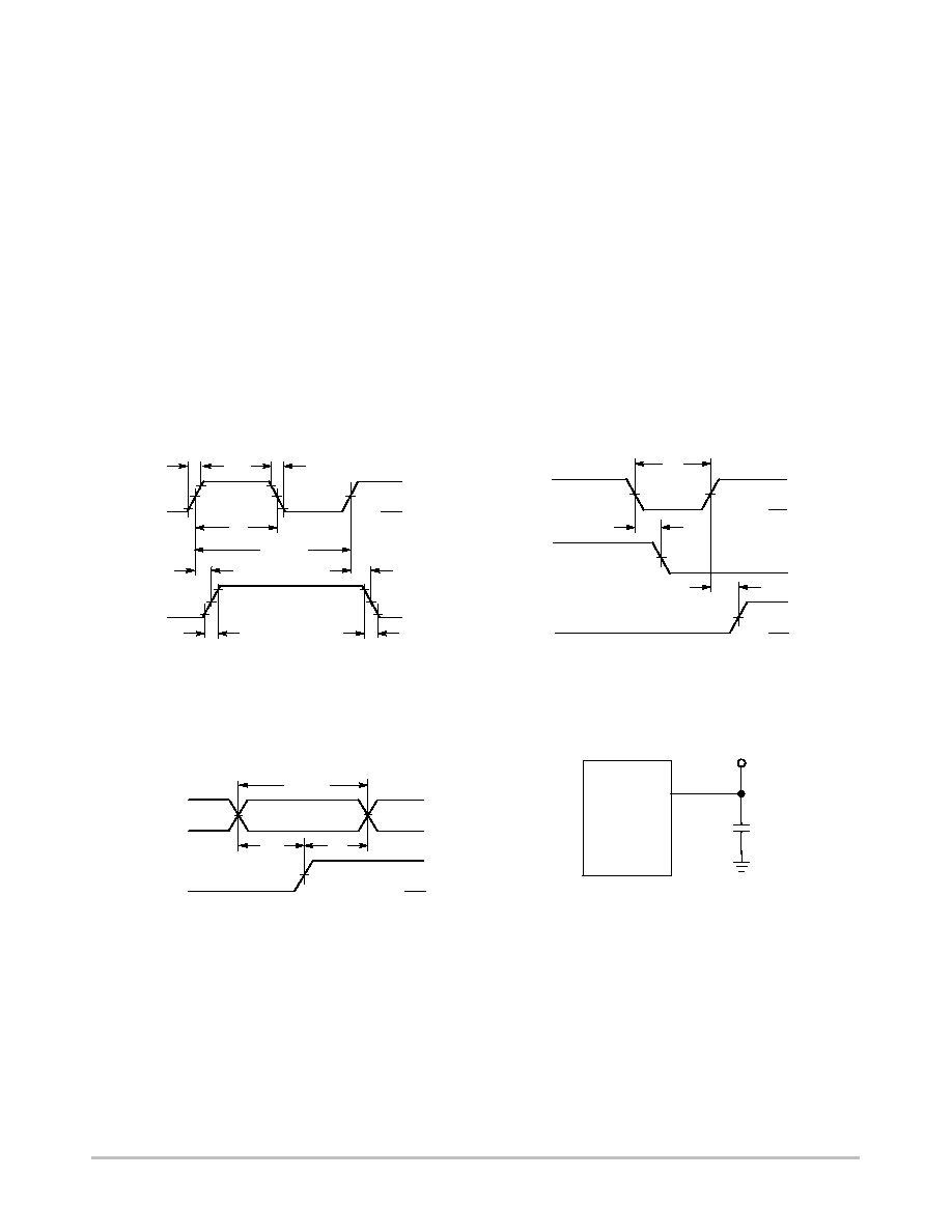
SWITCHING WAVEFORMS
tf
VCC
GND
90%
50%
10%
tw
tPLH
tPHL
CLOCK
Q
tTLH
tTHL
Figure 1.
RESET
trec
Figure 2.
tr
1/fmax
90%
50%
10%
VCC
GND
VCC
GND
Q
CLOCK
50%
50%
50%
tPHL
tw
A1 OR A2
Figure 3.
VCC
GND
VCC
GND
50%
50%
CLOCK
tsu
th
VALID
*Includes all probe and jig capacitance
CL*
TEST POINT
DEVICE
UNDER
TEST
OUTPUT
Figure 4. Test Circuit