®
Semiconductor Components Industries, LLC, 2001
May, 2001 Ł Rev. 5
1
Publication Order Number:
MC74AC244/D
MC74AC244, MC74ACT244
Octal Buffer/Line Driver
with 3-State Outputs
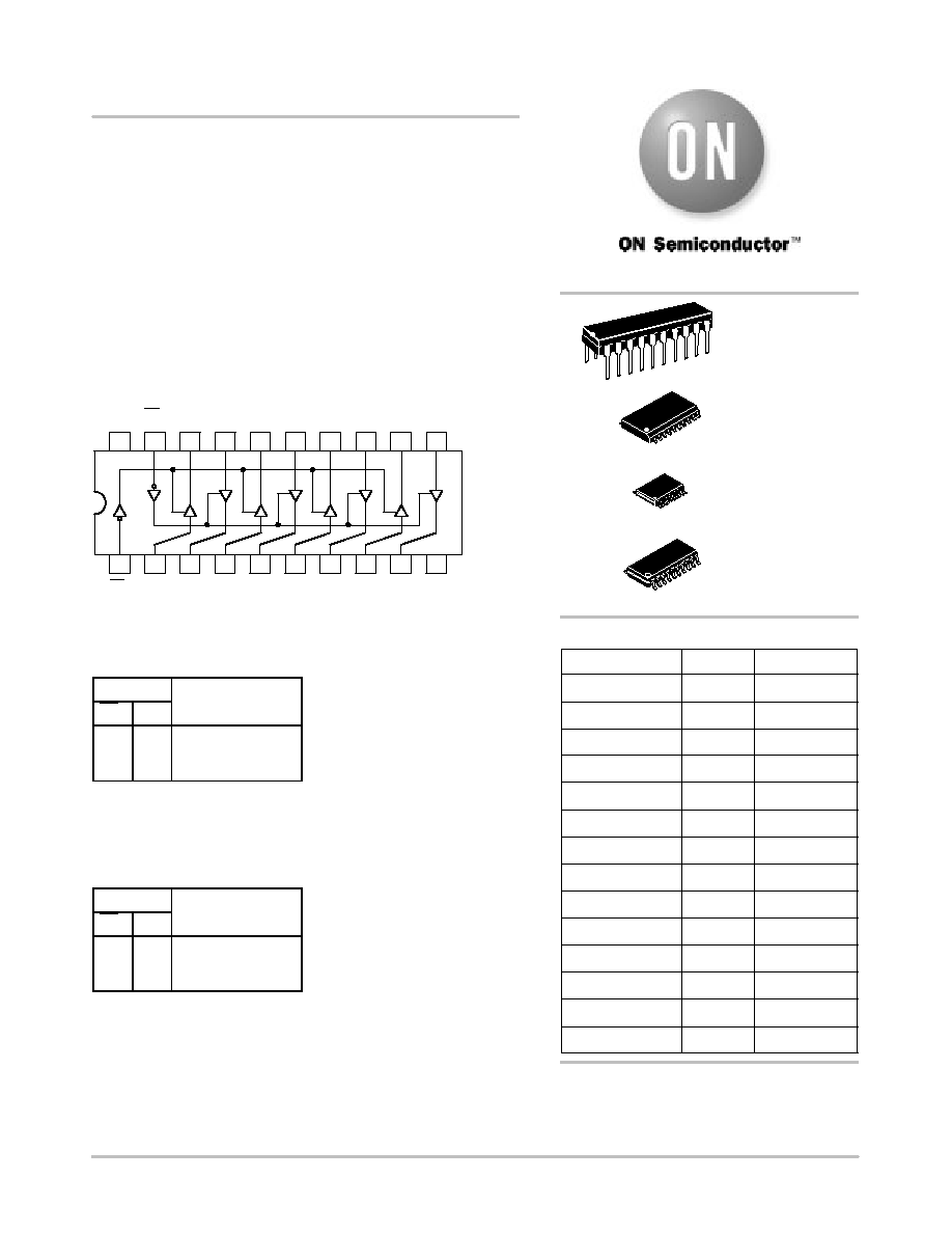
The MC74AC244/74ACT244 is an octal buffer and line driver
designed to be employed as a memory address driver, clock driver
and bus oriented transmitter/receiver which provides improved PC
board density.
Ę
3ŁState Outputs Drive Bus Lines or Buffer Memory Address
Registers
Ę
Outputs Source/Sink 24 mA
Ę
ACT244 Has TTL Compatible Inputs
19
20
18
17
16
15
14
2
1
3
4
5
6
7
VCC
13
8
12
9
11
10
OE2
OE1
GND
Figure 1. Pinout: 20ŁLead Packages Conductors
(Top View)
TRUTH TABLE
Inputs
Outputs
OE1
D
(Pins 12, 14, 16, 18)
L
L
L
L
H
H
H
X
Z
NOTE:
H = HIGH Voltage Level
L = LOW Voltage Level
X = Immaterial
Z = High Impedance
TRUTH TABLE
Inputs
Outputs
OE2
D
(Pins 3, 5, 7, 9)
L
L
L
L
H
H
H
X
Z
NOTE:
H = HIGH Voltage Level
L = LOW Voltage Level
X = Immaterial
Z = High Impedance
http://onsemi.com
1
20
PDIPŁ20
N SUFFIX
CASE 738
1
20
1
20
1
20
SOŁ20
DW SUFFIX
CASE 751
TSSOPŁ20
DT SUFFIX
CASE 948E
EIAJŁ20
M SUFFIX
CASE 967
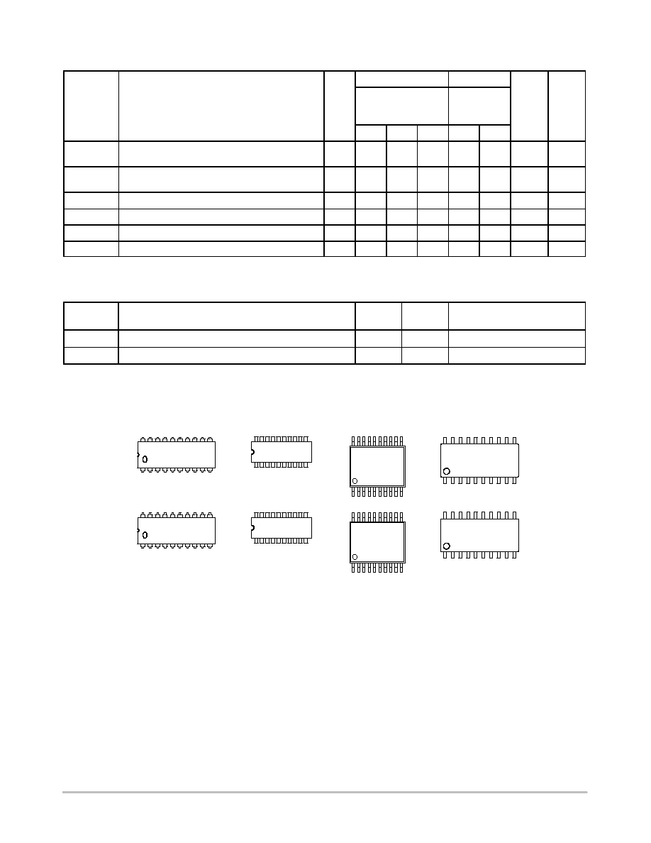
Device
Package
Shipping
ORDERING INFORMATION
MC74AC244N
PDIPŁ20
18 Units/Rail
MC74ACT244N
PDIPŁ20
18 Units/Rail
MC74AC244DW
SOICŁ20
38 Units/Rail
MC74AC244DWR2
SOICŁ20
1000 Tape & Reel
MC74ACT244DW
SOICŁ20
38 Units/Rail
MC74ACT244DWR2
SOICŁ20
1000 Tape & Reel
MC74AC244DT
TSSOPŁ20
75 Units/Rail
MC74AC244DTR2
TSSOPŁ20
2500 Tape & Reel
MC74ACT244DT
TSSOPŁ20
75 Units/Rail
MC74ACT244DTR2
TSSOPŁ20
2500 Tape & Reel
MC74AC244M
EIAJŁ20
40 Units/Rail
MC74AC244MEL
EIAJŁ20
2000 Tape & Reel
MC74ACT244M
EIAJŁ20
40 Units/Rail
MC74ACT244MEL
EIAJŁ20
2000 Tape & Reel
See general marking information in the device marking
section on page 5 of this data sheet.
DEVICE MARKING INFORMATION

MC74AC244, MC74ACT244
http://onsemi.com
2
MAXIMUM RATINGS*
Symbol
Parameter
Value
Unit
VCC
DC Supply Voltage (Referenced to GND)
Ł0.5 to +7.0
V
VIN
DC Input Voltage (Referenced to GND)
Ł0.5 to VCC +0.5
V
VOUT
DC Output Voltage (Referenced to GND)
Ł0.5 to VCC +0.5
V
IIN
DC Input Current, per Pin
▒
20
mA
IOUT
DC Output Sink/Source Current, per Pin
▒
50
mA
ICC
DC VCC or GND Current per Output Pin
▒
50
mA
Tstg
Storage Temperature
Ł65 to +150
░
C
*Maximum Ratings are those values beyond which damage to the device may occur. Functional operation should be restricted to the Recom-
mended Operating Conditions.
RECOMMENDED OPERATING CONDITIONS
Symbol
Parameter
Min
Typ
Max
Unit
V
Supply Voltage
AC
2.0
5.0
6.0
V
VCC
Supply Voltage
ACT
4.5
5.0
5.5
V
VIN, VOUT
DC Input Voltage, Output Voltage (Ref. to GND)
0
Ł
VCC
V
VCC @ 3.0 V
Ł
150
Ł
tr, tf
Input Rise and Fall Time (Note 1)
AC Devices except Schmitt Inputs
VCC @ 4.5 V
Ł
40
Ł
ns/V
r, f
AC Devices except Schmitt Inputs
VCC @ 5.5 V
Ł
25
Ł
t tf
Input Rise and Fall Time (Note 2)
VCC @ 4.5 V
Ł
10
Ł
ns/V
tr, tf
In ut Rise and Fall Time (Note 2)
ACT Devices except Schmitt Inputs
VCC @ 5.5 V
Ł
8.0
Ł
ns/V
TJ
Junction Temperature (PDIP)
Ł
Ł
140
░
C
TA
Operating Ambient Temperature Range
Ł40
25
85
░
C
IOH
Output Current Ł High
Ł
Ł
Ł24
mA
IOL
Output Current Ł Low
Ł
Ł
24
mA
1. VIN from 30% to 70% VCC; see individual Data Sheets for devices that differ from the typical input rise and fall times.
2. VIN from 0.8 V to 2.0 V; see individual Data Sheets for devices that differ from the typical input rise and fall times.
MC74AC244, MC74ACT244
http://onsemi.com
3
DC CHARACTERISTICS
74AC
74AC
Symbol
Parameter
VCC
(V)
TA = +25
░
C
TA =
Ł40
░
C to
+85
░
C
Unit
Conditions
Typ
Guaranteed Limits
VIH
Minimum High Level
3.0
1.5
2.1
2.1
VOUT = 0.1 V
g
Input Voltage
4.5
2.25
3.15
3.15
V
or VCC Ł 0.1 V
5.5
2.75
3.85
3.85
VIL
Maximum Low Level
3.0
1.5
0.9
0.9
VOUT = 0.1 V
Input Voltage
4.5
2.25
1.35
1.35
V
or VCC Ł 0.1 V
5.5
2.75
1.65
1.65
VOH
Minimum High Level
3.0
2.99
2.9
2.9
IOUT = Ł50
Ą
A
g
Output Voltage
4.5
4.49
4.4
4.4
V
5.5
5.49
5.4
5.4
*VIN = VIL or VIH
3.0
Ł
2.56
2.46
V
Ł12 mA
4.5
Ł
3.86
3.76
V
IOH
Ł24 mA
5.5
Ł
4.86
4.76
Ł24 mA
VOL
Maximum Low Level
3.0
0.002
0.1
0.1
IOUT = 50
Ą
A
Output Voltage
4.5
0.001
0.1
0.1
V
5.5
0.001
0.1
0.1
*VIN = VIL or VIH
3.0
Ł
0.36
0.44
V
12 mA
4.5
Ł
0.36
0.44
V
IOL
24 mA
5.5
Ł
0.36
0.44
24 mA
IIN
Maximum Input
5 5
Ł
▒
0 1
▒
1 0
Ą
A
VI = VCC GND
Leakage Current
5.5
Ł
▒
0.1
▒
1.0
Ą
A
VI = VCC, GND
IOZ
Maximum
VI (OE) = VIL, VIH
3ŁState
C
5.5
Ł
▒
0.5
▒
5.0
Ą
A
VI = VCC, GND
Current
VO = VCC, GND
IOLD
Minimum Dynamic
O t
t C
t
5.5
Ł
Ł
75
mA
VOLD = 1.65 V Max
IOHD
Output Current
5.5
Ł
Ł
Ł75
mA
VOHD = 3.85 V Min
ICC
Maximum Quiescent
5 5
Ł
8 0
80
Ą
A
VIN = VCC or GND
Q
Supply Current
5.5
Ł
8.0
80
Ą
A
VIN = VCC or GND
*All outputs loaded; thresholds on input associated with output under test.
Maximum test duration 2.0 ms, one output loaded at a time.
NOTE:
IIN and ICC @ 3.0 V are guaranteed to be less than or equal to the respective limit @ 5.5 V VCC.

MC74AC244, MC74ACT244
http://onsemi.com
4
AC CHARACTERISTICS (For Figures and Waveforms Ł See Section 3)
74AC
74AC
Symbol
Parameter
VCC*
(V)
TA = +25
░
C
CL = 50 pF
TA = Ł40
░
C
to +85
░
C
CL = 50 pF
Unit
Fig.
No.
Min
Typ
Max
Min
Max
tPLH
Propagation Delay
3.3
2.0
6.5
9.0
1.5
10.0
ns
3Ł5
tPLH
Data to Output
5.0
1.5
5.0
7.0
1.0
7.5
ns
3Ł5
tPHL
Propagation Delay
3.3
2.0
6.5
9.0
2.0
10.0
ns
3Ł5
tPHL
Data to Output
5.0
1.5
5.0
7.0
1.0
7.5
ns
3Ł5
tPZH
Output Enable Time
3.3
2.0
6.0
10.5
1.5
11.0
ns
3Ł7
tPZH
Output Enable Time
5.0
1.5
5.0
7.0
1.5
8.0
ns
3Ł7
tPZL
Output Enable Time
3.3
2.5
7.5
10.0
2.0
11.0
ns
3Ł8
tPZL
Output Enable Time
5.0
1.5
5.5
8.0
1.5
8.5
ns
3Ł8
tPHZ
Output Disable Time
3.3
3.0
7.0
10.0
1.5
10.5
ns
3Ł7
tPHZ
Output Disable Time
5.0
2.5
6.5
9.0
1.0
9.5
ns
3Ł7
tPLZ
Output Disable Time
3.3
2.5
7.5
10.5
2.5
11.5
ns
3Ł8
tPLZ
Output Disable Time
5.0
2.0
6.5
9.0
2.0
9.5
ns
3Ł8
*Voltage Range 3.3 V is 3.3 V
▒
0.3 V.
*Voltage Range 5.0 V is 5.0 V
▒
0.5 V.
DC CHARACTERISTICS
74ACT
74ACT
Symbol
Parameter
VCC
(V)
TA = +25
░
C
TA =
Ł40
░
C to
+85
░
C
Unit
Conditions
Typ
Guaranteed Limits
VIH
Minimum High Level
4.5
1.5
2.0
2.0
V
VOUT = 0.1 V
g
Input Voltage
5.5
1.5
2.0
2.0
V
or VCC Ł 0.1 V
VIL
Maximum Low Level
4.5
1.5
0.8
0.8
V
VOUT = 0.1 V
Input Voltage
5.5
1.5
0.8
0.8
V
or VCC Ł 0.1 V
VOH
Minimum High Level
4.5
4.49
4.4
4.4
V
IOUT = Ł50
Ą
A
g
Output Voltage
5.5
5.49
5.4
5.4
V
*VIN = VIL or VIH
4.5
Ł
3.86
3.76
V
IOH
Ł24 mA
5.5
Ł
4.86
4.76
IOH
Ł24 mA
VOL
Maximum Low Level
4.5
0.001
0.1
0.1
V
IOUT = 50
Ą
A
Output Voltage
5.5
0.001
0.1
0.1
V
*VIN = VIL or VIH
4.5
Ł
0.36
0.44
V
IOL
24 mA
5.5
Ł
0.36
0.44
IOL
24 mA
IIN
Maximum Input
5 5
Ł
▒
0 1
▒
1 0
Ą
A
VI = VCC GND
Leakage Current
5.5
Ł
▒
0.1
▒
1.0
Ą
A
VI = VCC, GND
ICCT
Additional Max. ICC/Input
5.5
0.6
Ł
1.5
mA
VI = VCC Ł 2.1 V
IOZ
Maximum
VI (OE) = VIL, VIH
3ŁState
C
5.5
Ł
▒
0.5
▒
5.0
Ą
A
VI = VCC, GND
Current
VO = VCC, GND
IOLD
Minimum Dynamic
O t
t C
t
5.5
Ł
Ł
75
mA
VOLD = 1.65 V Max
IOHD
Output Current
5.5
Ł
Ł
Ł75
mA
VOHD = 3.85 V Min
ICC
Maximum Quiescent
5 5
Ł
8 0
80
Ą
A
VIN = VCC or GND
Q
Supply Current
5.5
Ł
8.0
80
Ą
A
VIN = VCC or GND
*All outputs loaded; thresholds on input associated with output under test.
Maximum test duration 2.0 ms, one output loaded at a time.
MC74AC244, MC74ACT244
http://onsemi.com
5
AC CHARACTERISTICS (For Figures and Waveforms Ł See Section 3)
74ACT
74ACT
Symbol
Parameter
VCC*
(V)
TA = +25
░
C
CL = 50 pF
TA = Ł40
░
C
to +85
░
C
CL = 50 pF
Unit
Fig.
No.
Min
Typ
Max
Min
Max
tPLH
Propagation Delay
5 0
2 0
6 5
9 0
1 5
10 0
ns
3Ł5
tPLH
Pro agation Delay
Data to Output
5.0
2.0
6.5
9.0
1.5
10.0
ns
3Ł5
tPHL
Propagation Delay
5 0
2 0
7 0
9 0
1 5
10 0
ns
3Ł5
tPHL
Pro agation Delay
Data to Output
5.0
2.0
7.0
9.0
1.5
10.0
ns
3Ł5
tPZH
Output Enable Time
5.0
1.5
6.0
8.5
1.0
9.5
ns
3Ł7
tPZL
Output Enable Time
5.0
2.0
7.0
9.5
1.5
10.5
ns
3Ł8
tPHZ
Output Disable Time
5.0
2.0
7.0
9.5
1.5
10.5
ns
3Ł7
tPLZ
Output Disable Time
5.0
2.5
7.5
10.0
2.0
10.5
ns
3Ł8
*Voltage Range 5.0 V is 5.0 V
▒
0.5 V.
CAPACITANCE
Symbol
Parameter
Value
Typ
Unit
Test Conditions
CIN
Input Capacitance
4.5
pF
VCC = 5.0 V
CPD
Power Dissipation Capacitance
45
pF
VCC = 5.0 V
AC
244
ALYW
AC244
AWLYYWW
MC74AC244N
AWLYYWW
74AC244
AWLYWW
MARKING DIAGRAMS
PDIPŁ20
SOŁ20
TSSOPŁ20
EIAJŁ20
ACT
244
ALYW
ACT244
AWLYYWW
MC74ACT244N
AWLYYWW
74ACT244
AWLYWW
A
= Assembly Location
WL, L
= Wafer Lot
YY, Y
= Year
WW, W = Work Week