
ˋ
Semiconductor Components Industries, LLC, 2001
May, 2001 Ù Rev. 5
1
Publication Order Number:
MC74AC109/D
MC74AC109, MC74ACT109
Dual JK Positive
Edge-Triggered Flip-Flop
The MC74AC109/74ACT109 consists of two highÙspeed
completely independent transition clocked JK flipÙflops. The
clocking operation is independent of rise and fall times of the clock
waveform. The JK design allows operation as a D flipÙflop (refer to
MC74AC74/74ACT74 data sheet) by connecting the J and K inputs
together.
Asynchronous Inputs:
LOW input to SD (Set) sets Q to HIGH level
LOW input to CD (Clear) sets Q to LOW level
Clear and Set are independent of clock
Simultaneous LOW on CD and SD makes both Q and Q HIGH
ñ
Outputs Source/Sink 24 mA
ñ
ACT109 Has TTL Compatible Inputs
15
16
14
13
12
11
10
2
1
3
4
5
6
7
VCC
9
8
CD2
J2
K2 CP2 SD2 Q2
Q2
CD1
J1
K1 CP1 SD1 Q1
Q1 GND
J1
K1
CP1
SD1
Q1
Q1
CD
J
K
CP
SD
Q
Q
CD1
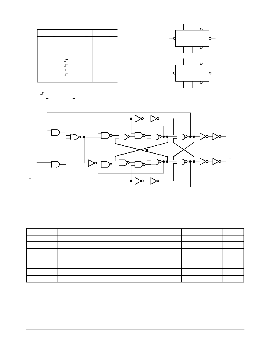
Figure 1. Pinout; 16ÙLead Packages Conductors
(Top View)
PIN ASSIGNMENT
PIN
FUNCTION
J1, J2, K1, K2
Data Inputs
CP1, CP2
Clock Pulse Inputs
CD1, CD2
Direct Clear Inputs
SD1, SD2
Direct Set Inputs
Q1, Q2, Q1, Q2
Outputs
http://onsemi.com
DIPÙ16
N SUFFIX
CASE 648
1
16
SOÙ16
D SUFFIX
CASE 751B
1
16
Device
Package
Shipping
ORDERING INFORMATION
MC74AC109N
PDIPÙ16
25 Units/Rail
MC74AC109D
SOICÙ16
48 Units/Rail
MC74AC109DR2
2500 Tape & Reel
TSSOPÙ16
DT SUFFIX
CASE 948F
MC74AC109DT
TSSOPÙ16
96 Units/Rail
MC74AC109DTR2
TSSOPÙ16
SOICÙ16
2500 Tape & Reel
MC74ACT109N
PDIPÙ16
25 Units/Rail
MC74ACT109D
SOICÙ16
48 Units/Rail
MC74ACT109DR2
2500 Tape & Reel
MC74ACT109DT
TSSOPÙ16
96 Units/Rail
MC74ACT109DTR2 TSSOPÙ16
SOICÙ16
2500 Tape & Reel
1
16
See general marking information in the device marking
section on page 6 of this data sheet.
DEVICE MARKING INFORMATION
1
16
EIAJÙ16
M SUFFIX
CASE 966
MC74AC109M
EIAJÙ16
MC74AC109MEL
EIAJÙ16
2000 Tape & Reel
MC74ACT109M
EIAJÙ16
MC74ACT109MEL
EIAJÙ16
2000 Tape & Reel
50 Units/Rail
50 Units/Rail
MC74AC109, MC74ACT109
http://onsemi.com
2
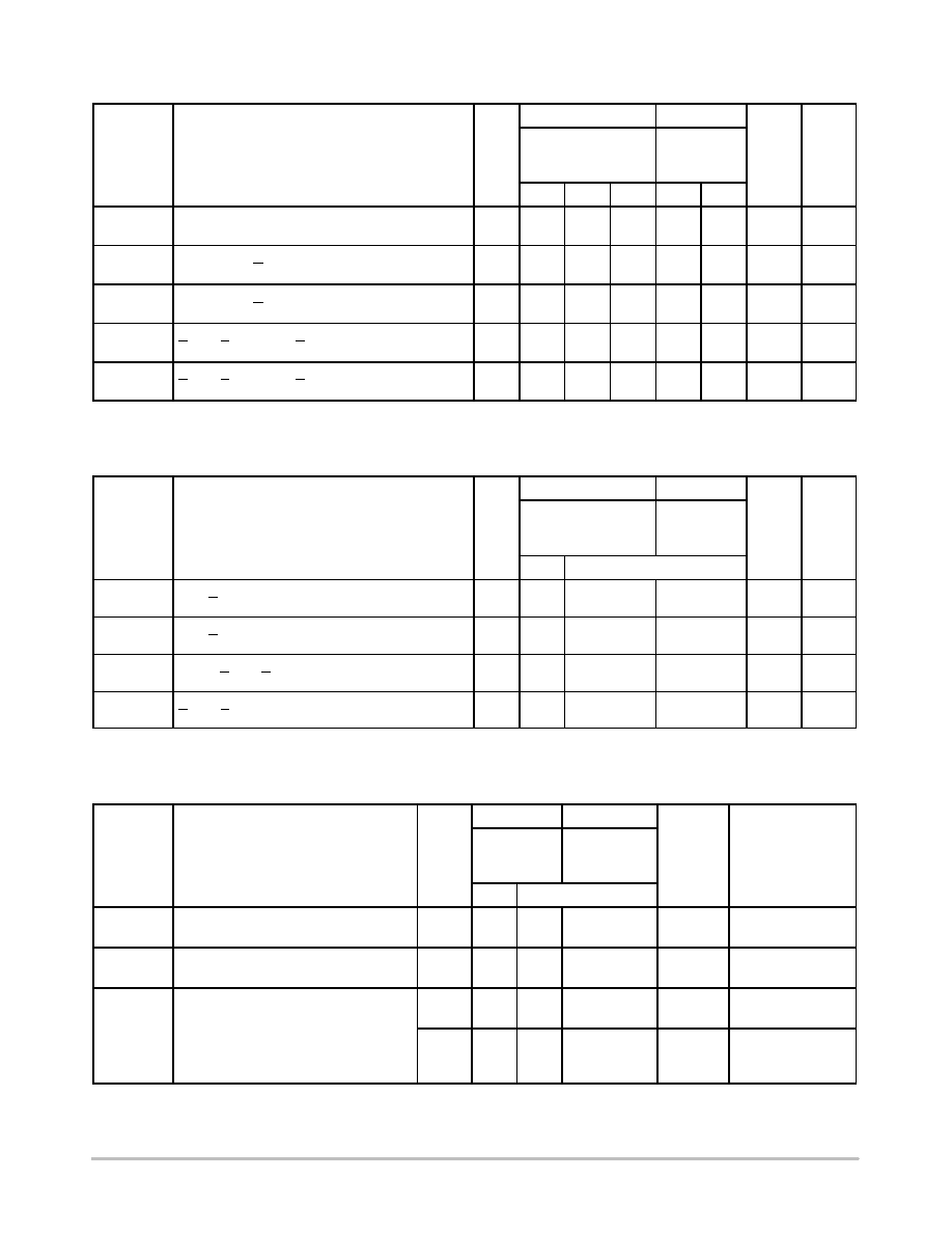
TRUTH TABLE
Inputs
Outputs
SD
CD
CP
J
K
Q
Q
L
H
X
X
X
H
L
H
L
X
X
X
L
H
L
L
X
X
X
H
H
H
H
L
L
L
H
H
H
H
L
Toggle
H
H
L
H
Q0
Q0Ù
H
H
H
H
H
L
H
H
L
X
X
Q0
Q0Ù
H = HIGH Voltage Level
L = LOW Voltage Level
= LOWÙtoÙHIGH Clock Transition
X = Immaterial
Q0(Q0) = Previous Q0(Q0) before
LOWÙtoÙHIGH Transition of Clock
Figure 2. Logic Symbol
SD
Q
J
CP
Q
CD
K
SD
Q
J
CP
Q
CD
K
SD
K
CP
J
CD
Q
Q
NOTE:
This diagram is provided only for the understanding of logic
operations and should not be used to estimate propagation delays.
Figure 3. Logic Diagram
(One Half Shown)
MAXIMUM RATINGS*
Symbol
Parameter
Value
Unit
VCC
DC Supply Voltage (Referenced to GND)
Ù0.5 to +7.0
V
VIN
DC Input Voltage (Referenced to GND)
Ù0.5 to VCC +0.5
V
VOUT
DC Output Voltage (Referenced to GND)
Ù0.5 to VCC +0.5
V
IIN
DC Input Current, per Pin
Ý
20
mA
IOUT
DC Output Sink/Source Current, per Pin
Ý
50
mA
ICC
DC VCC or GND Current per Output Pin
Ý
50
mA
Tstg
Storage Temperature
Ù65 to +150
¯
C
*Maximum Ratings are those values beyond which damage to the device may occur. Functional operation should be restricted to the Recom-
mended Operating Conditions.

MC74AC109, MC74ACT109
http://onsemi.com
3
RECOMMENDED OPERATING CONDITIONS
Symbol
Parameter
Min
Typ
Max
Unit
V
Supply Voltage
AC
2.0
5.0
6.0
V
VCC
Supply Voltage
ACT
4.5
5.0
5.5
V
VIN, VOUT
DC Input Voltage, Output Voltage (Ref. to GND)
0
Ù
VCC
V
VCC @ 3.0 V
Ù
150
Ù
tr, tf
Input Rise and Fall Time (Note 1)
AC Devices except Schmitt Inputs
VCC @ 4.5 V
Ù
40
Ù
ns/V
r, f
AC Devices except Schmitt Inputs
VCC @ 5.5 V
Ù
25
Ù
t tf
Input Rise and Fall Time (Note 2)
VCC @ 4.5 V
Ù
10
Ù
ns/V
tr, tf
In ut Rise and Fall Time (Note 2)
ACT Devices except Schmitt Inputs
VCC @ 5.5 V
Ù
8.0
Ù
ns/V
TJ
Junction Temperature (PDIP)
Ù
Ù
140
¯
C
TA
Operating Ambient Temperature Range
Ù40
25
85
¯
C
IOH
Output Current Ù High
Ù
Ù
Ù24
mA
IOL
Output Current Ù Low
Ù
Ù
24
mA
1. VIN from 30% to 70% VCC; see individual Data Sheets for devices that differ from the typical input rise and fall times.
2. VIN from 0.8 V to 2.0 V; see individual Data Sheets for devices that differ from the typical input rise and fall times.
DC CHARACTERISTICS
74AC
74AC
Symbol
Parameter
VCC
(V)
TA = +25
¯
C
TA =
Ù40
¯
C to
+85
¯
C
Unit
Conditions
Typ
Guaranteed Limits
VIH
Minimum High Level
3.0
1.5
2.1
2.1
VOUT = 0.1 V
g
Input Voltage
4.5
2.25
3.15
3.15
V
or VCC Ù 0.1 V
5.5
2.75
3.85
3.85
VIL
Maximum Low Level
3.0
1.5
0.9
0.9
VOUT = 0.1 V
Input Voltage
4.5
2.25
1.35
1.35
V
or VCC Ù 0.1 V
5.5
2.75
1.65
1.65
VOH
Minimum High Level
3.0
2.99
2.9
2.9
IOUT = Ù50
ç
A
g
Output Voltage
4.5
4.49
4.4
4.4
V
5.5
5.49
5.4
5.4
*VIN = VIL or VIH
3.0
Ù
2.56
2.46
V
Ù12 mA
4.5
Ù
3.86
3.76
V
IOH
Ù24 mA
5.5
Ù
4.86
4.76
Ù24 mA
VOL
Maximum Low Level
3.0
0.002
0.1
0.1
IOUT = 50
ç
A
Output Voltage
4.5
0.001
0.1
0.1
V
5.5
0.001
0.1
0.1
*VIN = VIL or VIH
3.0
Ù
0.36
0.44
V
12 mA
4.5
Ù
0.36
0.44
V
IOL
24 mA
5.5
Ù
0.36
0.44
24 mA
IIN
Maximum Input
5 5
Ù
Ý
0 1
Ý
1 0
ç
A
VI = VCC GND
Leakage Current
5.5
Ù
Ý
0.1
Ý
1.0
ç
A
VI = VCC, GND
IOLD
Minimum Dynamic
O t
t C
t
5.5
Ù
Ù
75
mA
VOLD = 1.65 V Max
IOHD
Output Current
5.5
Ù
Ù
Ù75
mA
VOHD = 3.85 V Min
ICC
Maximum Quiescent
5 5
Ù
4 0
40
ç
A
VIN = VCC or GND
Q
Supply Current
5.5
Ù
4.0
40
ç
A
VIN = VCC or GND
*All outputs loaded; thresholds on input associated with output under test.
Maximum test duration 2.0 ms, one output loaded at a time.
NOTE:
IIN and ICC @ 3.0 V are guaranteed to be less than or equal to the respective limit @ 5.5 V VCC.
MC74AC109, MC74ACT109
http://onsemi.com
4
AC CHARACTERISTICS
(For Figures and Waveforms Ù See Section 3 of the ON Semiconductor FACT Data Book, DL138/D)
74AC
74AC
Symbol
Parameter
VCC*
(V)
TA = +25
¯
C
CL = 50 pF
TA = Ù40
¯
C
to +85
¯
C
CL = 50 pF
Unit
Fig.
No.
Min
Typ
Max
Min
Max
fmax
Maximum Clock
3.3
125
Ù
Ù
100
Ù
MHz
3Ù3
fmax
Frequency
5.0
150
Ù
Ù
125
Ù
MHz
3Ù3
tPLH
Propagation Delay
3.3
4.0
Ù
13.5
3.5
16.0
ns
3Ù6
tPLH
g
y
CPn to Qn or Qn
5.0
2.5
Ù
10.0
2.0
10.5
ns
3Ù6
tPHL
Propagation Delay
3.3
3.0
Ù
14.0
3.0
14.5
ns
3Ù6
tPHL
g
y
CPn to Qn or Qn
5.0
2.0
Ù
10.0
1.5
10.5
ns
3Ù6
tPLH
Propagation Delay
3.3
3.0
Ù
12.0
2.5
13.0
ns
3Ù6
tPLH
g
y
CDn or SDn to Qn or Qn
5.0
2.5
Ù
9.0
2.0
10.0
ns
3Ù6
tPHL
Propagation Delay
3.3
3.0
Ù
12.0
3.0
13.5
ns
3Ù6
tPHL
g
y
CDn or SDn to Qn or Qn
5.0
2.0
Ù
9.5
2.0
10.5
ns
3Ù6
*Voltage Range 3.3 V is 3.3 V
Ý
0.3 V.
*Voltage Range 5.0 V is 5.0 V
Ý
0.5 V.
AC OPERATING REQUIREMENTS
74AC
74AC
Symbol
Parameter
VCC*
(V)
TA = +25
¯
C
CL = 50 pF
TA = Ù40
¯
C
to +85
¯
C
CL = 50 pF
Unit
Fig.
No.
Typ
Guaranteed Minimum
ts
SetÙup Time, HIGH or LOW
3.3
Ù
6.5
7.5
ns
3Ù9
ts
Set u Time, HIGH or LOW
Jn or Kn to CPn
3.3
5.0
Ù
6.5
4.5
7.5
5.0
ns
3Ù9
th
Hold Time, HIGH or LOW
3.3
Ù
0
0
ns
3Ù9
th
Hold Time, HIGH or LOW
Jn or Kn to CPn
3.3
5.0
Ù
0
0.5
0
0.5
ns
3Ù9
tw
Pulse Width
3.3
Ù
4.0
4.5
ns
3Ù6
tw
Pulse Width
CPn or CDn or SDn
3.3
5.0
Ù
4.0
3.5
4.5
3.5
ns
3Ù6
trec
Recovery TIme
3.3
Ù
0
0
ns
3Ù9
trec
Recovery TIme
CDn or SDn to CP
3.3
5.0
Ù
0
0
0
0
ns
3Ù9
*Voltage Range 3.3 V is 3.3 V
Ý
0.3 V.
*Voltage Range 5.0 V is 5.0 V
Ý
0.5 V.
DC CHARACTERISTICS
74ACT
74ACT
Symbol
Parameter
VCC
(V)
TA = +25
¯
C
TA =
Ù40
¯
C to
+85
¯
C
Unit
Conditions
Typ
Guaranteed Limits
VIH
Minimum High Level
4.5
1.5
2.0
2.0
V
VOUT = 0.1 V
g
Input Voltage
5.5
1.5
2.0
2.0
V
or VCC Ù 0.1 V
VIL
Maximum Low Level
4.5
1.5
0.8
0.8
V
VOUT = 0.1 V
Input Voltage
5.5
1.5
0.8
0.8
V
or VCC Ù 0.1 V
VOH
Minimum High Level
4.5
4.49
4.4
4.4
V
IOUT = Ù50
ç
A
g
Output Voltage
5.5
5.49
5.4
5.4
V
*VIN = VIL or VIH
4.5
Ù
3.86
3.76
V
IOH
Ù24 mA
5.5
Ù
4.86
4.76
IOH
Ù24 mA
*All outputs loaded; thresholds on input associated with output under test.
Maximum test duration 2.0 ms, one output loaded at a time.

MC74AC109, MC74ACT109
http://onsemi.com
5
DC CHARACTERISTICS (continued)
Symbol
Conditions
Unit
74ACT
74ACT
VCC
(V)
Parameter
Symbol
Conditions
Unit
TA =
Ù40
¯
C to
+85
¯
C
TA = +25
¯
C
VCC
(V)
Parameter
Symbol
Conditions
Unit
Guaranteed Limits
Typ
VCC
(V)
Parameter
VOL
Maximum Low Level
4.5
0.001
0.1
0.1
V
IOUT = 50
ç
A
Output Voltage
5.5
0.001
0.1
0.1
V
*VIN = VIL or VIH
4.5
Ù
0.36
0.44
V
IOL
24 mA
5.5
Ù
0.36
0.44
IOL
24 mA
IIN
Maximum Input
5 5
Ù
Ý
0 1
Ý
1 0
ç
A
VI = VCC GND
Leakage Current
5.5
Ù
Ý
0.1
Ý
1.0
ç
A
VI = VCC, GND
ICCT
Additional Max. ICC/Input
5.5
0.6
Ù
1.5
mA
VI = VCC Ù 2.1 V
IOLD
Minimum Dynamic
O t
t C
t
5.5
Ù
Ù
75
mA
VOLD = 1.65 V Max
IOHD
Output Current
5.5
Ù
Ù
Ù75
mA
VOHD = 3.85 V Min
ICC
Maximum Quiescent
5 5
Ù
4 0
40
ç
A
VIN = VCC or GND
Q
Supply Current
5.5
Ù
4.0
40
ç
A
VIN = VCC or GND
*All outputs loaded; thresholds on input associated with output under test.
Maximum test duration 2.0 ms, one output loaded at a time.
AC CHARACTERISTICS
(For Figures and Waveforms Ù See Section 3 of the ON Semiconductor FACT Data Book, DL138/D)
74ACT
74ACT
Symbol
Parameter
VCC*
(V)
TA = +25
¯
C
CL = 50 pF
TA = Ù40
¯
C
to +85
¯
C
CL = 50 pF
Unit
Fig.
No.
Min
Typ
Max
Min
Max
fmax
Maximum Clock
5 0
145
Ù
Ù
125
Ù
MHz
3Ù3
fmax
Maximum Clock
Frequency
5.0
145
Ù
Ù
125
Ù
MHz
3Ù3
tPLH
Propagation Delay
5 0
4 0
Ù
11 0
3 5
13 0
ns
3Ù6
tPLH
Pro agation Delay
CPn to Qn or Qn
5.0
4.0
Ù
11.0
3.5
13.0
ns
3Ù6
tPHL
Propagation Delay
5 0
3 0
Ù
10 0
2 5
11 5
ns
3Ù6
tPHL
Pro agation Delay
CPn to Qn or Qn
5.0
3.0
Ù
10.0
2.5
11.5
ns
3Ù6
tPLH
Propagation Delay
5 0
2 5
Ù
9 5
2 0
10 5
ns
3Ù6
tPLH
Pro agation Delay
CDn or SDn to Qn or Qn
5.0
2.5
Ù
9.5
2.0
10.5
ns
3Ù6
tPHL
Propagation Delay
5 0
2 5
Ù
10 0
2 0
11 5
ns
3Ù6
tPHL
Pro agation Delay
CDn or SDn to Qn or Qn
5.0
2.5
Ù
10.0
2.0
11.5
ns
3Ù6
*Voltage Range 5.0 V is 5.0 V
Ý
0.5 V.
AC OPERATING REQUIREMENTS
74ACT
74ACT
Symbol
Parameter
VCC*
(V)
TA = +25
¯
C
CL = 50 pF
TA = Ù40
¯
C
to +85
¯
C
CL = 50 pF
Unit
Fig.
No.
Typ
Guaranteed Minimum
ts
SetÙup Time, HIGH or LOW
5 0
Ù
2 0
2 5
ns
3Ù9
ts
Set u Time, HIGH or LOW
Jn or Kn to CPn
5.0
Ù
2.0
2.5
ns
3Ù9
th
Hold Time, HIGH or LOW
5 0
Ù
2 0
2 0
ns
3Ù9
th
Hold Time, HIGH or LOW
Jn or Kn to CPn
5.0
Ù
2.0
2.0
ns
3Ù9
tw
Pulse Width
5 0
Ù
5 0
6 0
ns
3Ù6
tw
Pulse Width
CPn or CDn or SDn
5.0
Ù
5.0
6.0
ns
3Ù6
*Voltage Range 5.0 V is 5.0 V
Ý
0.5 V.