©
Semiconductor Components Industries, LLC, 2001
May, 2001 Rev. 5
1
Publication Order Number:
MC74AC04/D
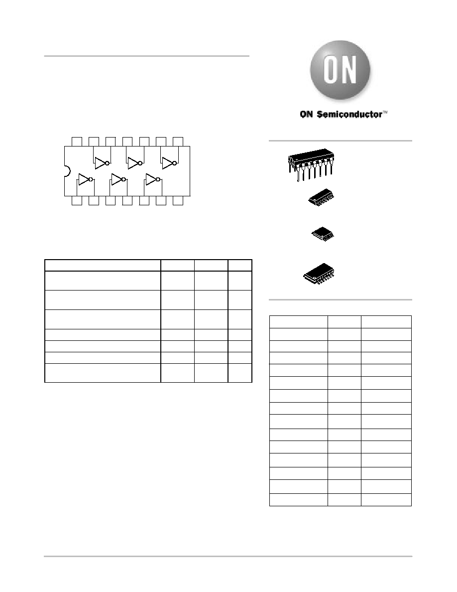
MC74AC04, MC74ACT04
Hex Inverter
·
Outputs Source/Sink 24 mA
·
ACT04 Has TTL Compatible Inputs
13
14
12
11
10
9
8
2
1
3
4
5
6
7
GND
VCC
Figure 1. Pinout: 14Lead Packages Conductors
(Top View)
MAXIMUM RATINGS*
Rating
Symbol
Value
Unit
DC Supply Voltage (Referenced to GND)
VCC
0.5 to
+7.0
V
DC Input Voltage (Referenced to GND)
Vin
0.5 to
VCC +0.5
V
DC Output Voltage (Referenced to GND)
Vout
0.5 to
VCC +0.5
V
DC Input Current, per Pin
Iin
±
20
mA
DC Output Sink/Source Current, per Pin
Iout
±
50
mA
DC VCC or GND Current per Output Pin
ICC
±
50
mA
Storage Temperature
Tstg
65 to
+150
°
C
*Maximum Ratings are those values beyond which damage to the device may
occur. Functional operation should be restricted to the Recommended Operating
Conditions.
TSSOP14
DT SUFFIX
CASE 948G
1
14
EIAJ14
M SUFFIX
CASE 965
1
14
SO14
D SUFFIX
CASE 751A
http://onsemi.com
1
14
1
14
PDIP14
N SUFFIX
CASE 646
Device
Package
Shipping
ORDERING INFORMATION
MC74AC04DT
TSSOP14
96 Units/Rail
MC74AC04DTR2
TSSOP14 2500 Tape & Reel
MC74ACT04DT
TSSOP14
96 Units/Rail
MC74ACT04DTR2
TSSOP14 2500 Tape & Reel
MC74AC04N
PDIP14
25 Units/Rail
MC74AC04D
SOIC14
55 Units/Rail
MC74ACT04N
PDIP14
25 Units/Rail
MC74AC04DR2
SOIC14
2500 Tape & Reel
MC74ACT04D
SOIC14
55 Units/Rail
MC74ACT04DR2
SOIC14
2500 Tape & Reel
MC74AC04M
EIAJ14
50 Units/Rail
MC74AC04MEL
EIAJ14
2000 Tape & Reel
MC74ACT04M
EIAJ14
50 Units/Rail
MC74ACT04MEL
EIAJ14
2000 Tape & Reel
See general marking information in the device marking
section on page 5 of this data sheet.
DEVICE MARKING INFORMATION

MC74AC04, MC74ACT04
http://onsemi.com
2
RECOMMENDED OPERATING CONDITIONS
Symbol
Parameter
Min
Typ
Max
Unit
V
Supply Voltage
AC
2.0
5.0
6.0
V
VCC
Supply Voltage
ACT
4.5
5.0
5.5
V
Vin, Vout
DC Input Voltage, Output Voltage (Ref. to GND)
0
VCC
V
VCC @ 3.0 V
150
tr, tf
Input Rise and Fall Time (Note 1)
AC Devices except Schmitt Inputs
VCC @ 4.5 V
40
ns/V
r, f
AC Devices except Schmitt Inputs
VCC @ 5.5 V
25
t tf
Input Rise and Fall Time (Note 2)
VCC @ 4.5 V
10
ns/V
tr, tf
In ut Rise and Fall Time (Note 2)
ACT Devices except Schmitt Inputs
VCC @ 5.5 V
8.0
ns/V
TJ
Junction Temperature (PDIP)
140
°
C
TA
Operating Ambient Temperature Range
40
25
85
°
C
IOH
Output Current High
24
mA
IOL
Output Current Low
24
mA
1. Vin from 30% to 70% VCC; see individual Data Sheets for devices that differ from the typical input rise and fall times.
2. Vin from 0.8 V to 2.0 V; see individual Data Sheets for devices that differ from the typical input rise and fall times.
DC CHARACTERISTICS
74AC
74AC
Symbol
Parameter
VCC
(V)
TA = +25
°
C
TA =
40
°
C to
+85
°
C
Unit
Conditions
Typ
Guaranteed Limits
VIH
Minimum High Level
3.0
1.5
2.1
2.1
VOUT = 0.1 V
g
Input Voltage
4.5
2.25
3.15
3.15
V
or VCC 0.1 V
5.5
2.75
3.85
3.85
VIL
Maximum Low Level
3.0
1.5
0.9
0.9
VOUT = 0.1 V
Input Voltage
4.5
2.25
1.35
1.35
V
or VCC 0.1 V
5.5
2.75
1.65
1.65
VOH
Minimum High Level
3.0
2.99
2.9
2.9
IOUT = 50
µ
A
g
Output Voltage
4.5
4.49
4.4
4.4
V
5.5
5.49
5.4
5.4
*VIN = VIL or VIH
3.0
2.56
2.46
V
12 mA
4.5
3.86
3.76
V
IOH
24 mA
5.5
4.86
4.76
24 mA
VOL
Maximum Low Level
3.0
0.002
0.1
0.1
IOUT = 50
µ
A
Output Voltage
4.5
0.001
0.1
0.1
V
5.5
0.001
0.1
0.1
*VIN = VIL or VIH
3.0
0.36
0.44
V
12 mA
4.5
0.36
0.44
V
IOL
24 mA
5.5
0.36
0.44
24 mA
IIN
Maximum Input
5 5
±
0 1
±
1 0
µ
A
VI = VCC GND
Leakage Current
5.5
±
0.1
±
1.0
µ
A
VI = VCC, GND
IOLD
Minimum Dynamic
O t
t C
t
5.5
75
mA
VOLD = 1.65 V Max
IOHD
Output Current
5.5
75
mA
VOHD = 3.85 V Min
ICC
Maximum Quiescent
5 5
4 0
40
µ
A
VIN = VCC or GND
Q
Supply Current
5.5
4.0
40
µ
A
VIN = VCC or GND
*All outputs loaded; thresholds on input associated with output under test.
Maximum test duration 2.0 ms, one output loaded at a time.
NOTE:
IIN and ICC @ 3.0 V are guaranteed to be less than or equal to the respective limit @ 5.5 V VCC.
MC74AC04, MC74ACT04
http://onsemi.com
3
AC CHARACTERISTICS
(For Figures and Waveforms See Section 3 of the ON Semiconductor FACT Data Book, DL138/D)
74AC
74AC
Symbol
Parameter
VCC*
(V)
TA = +25
°
C
CL = 50 pF
TA = 40
°
C
to +85
°
C
CL = 50 pF
Unit
Fig.
No.
Min
Typ
Max
Min
Max
tPLH
Propagation Delay
3.3
1.5
4.5
9.0
1.0
10
ns
35
tPLH
Propagation Delay
5.0
1.5
4.0
7.0
1.0
7.5
ns
35
tPHL
Propagation Delay
3.3
1.5
4.5
8.5
1.0
9.5
ns
35
tPHL
Propagation Delay
5.0
1.5
3.5
6.5
1.0
7.0
ns
35
*Voltage Range 3.3 V is 3.3 V
±
0.3 V.
Voltage Range 5.0 V is 5.0 V
±
0.5 V.
DC CHARACTERISTICS
74ACT
74ACT
Symbol
Parameter
VCC
(V)
TA = +25
°
C
TA =
40
°
C to
+85
°
C
Unit
Conditions
Typ
Guaranteed Limits
VIH
Minimum High Level
4.5
1.5
2.0
2.0
V
VOUT = 0.1 V
g
Input Voltage
5.5
1.5
2.0
2.0
V
or VCC 0.1 V
VIL
Maximum Low Level
4.5
1.5
0.8
0.8
V
VOUT = 0.1 V
Input Voltage
5.5
1.5
0.8
0.8
V
or VCC 0.1 V
VOH
Minimum High Level
4.5
4.49
4.4
4.4
V
IOUT = 50
µ
A
g
Output Voltage
5.5
5.49
5.4
5.4
V
*VIN = VIL or VIH
4.5
3.86
3.76
V
IOH
24 mA
5.5
4.86
4.76
IOH
24 mA
VOL
Maximum Low Level
4.5
0.001
0.1
0.1
V
IOUT = 50
µ
A
Output Voltage
5.5
0.001
0.1
0.1
V
*VIN = VIL or VIH
4.5
0.36
0.44
V
IOL
24 mA
5.5
0.36
0.44
IOL
24 mA
IIN
Maximum Input
5 5
±
0 1
±
1 0
µ
A
VI = VCC GND
Leakage Current
5.5
±
0.1
±
1.0
µ
A
VI = VCC, GND
ICCT
Additional Max. ICC/Input
5.5
0.6
1.5
mA
VI = VCC 2.1 V
IOLD
Minimum Dynamic
O t
t C
t
5.5
75
mA
VOLD = 1.65 V Max
IOHD
Output Current
5.5
75
mA
VOHD = 3.85 V Min
ICC
Maximum Quiescent
5 5
4 0
40
µ
A
VIN = VCC or GND
Q
Supply Current
5.5
4.0
40
µ
A
VIN = VCC or GND
*All outputs loaded; thresholds on input associated with output under test.
Maximum test duration 2.0 ms, one output loaded at a time.
MC74AC04, MC74ACT04
http://onsemi.com
4
AC CHARACTERISTICS
(For Figures and Waveforms See Section 3 of the ON Semiconductor FACT Data Book, DL138/D)
74ACT
74ACT
Symbol
Parameter
VCC*
(V)
TA = +25
°
C
CL = 50 pF
TA = 40
°
C
to +85
°
C
CL = 50 pF
Unit
Fig.
No.
Min
Typ
Max
Min
Max
tPLH
Propagation Delay
5.0
1.5
8.5
1.0
9.0
ns
36
tPHL
Propagation Delay
5.0
1.5
8.0
1.0
8.5
ns
36
*Voltage Range 5.0 V is 5.0 V
±
0.5 V.
CAPACITANCE
Symbol
Parameter
Value
Typ
Unit
Test Conditions
CIN
Input Capacitance
4.5
pF
VCC = 5.0 V
CPD
Power Dissipation Capacitance
30
pF
VCC = 5.0 V
MC74AC04, MC74ACT04
http://onsemi.com
5
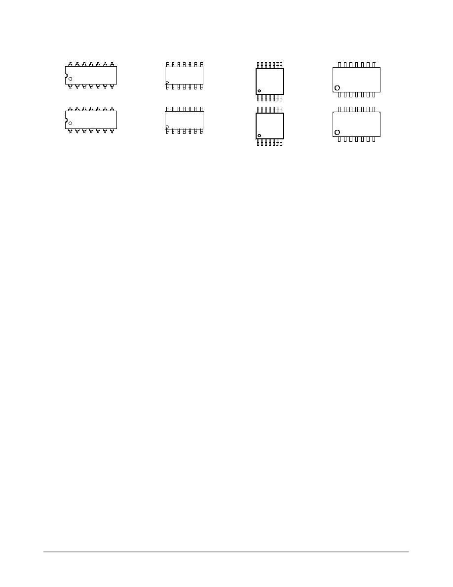
MARKING DIAGRAMS
A
= Assembly Location
WL, L
= Wafer Lot
YY, Y
= Year
WW, W = Work Week
PDIP14
SO14
TSSOP14
MC74AC04N
AWLYYWW
AC04
AWLYWW
AC
04
ALYW
ACT
04
ALYW
ACT04
AWLYWW
MC74ACT04N
AWLYYWW
74AC04
ALYW
EIAJ14
74ACT04
ALYW