ę
Semiconductor Components Industries, LLC, 2000
April, 2000 ş Rev. 1
1
Publication Order Number:
MC34151/D
MC34151, MC33151
High Speed Dual
MOSFET Drivers
The MC34151/MC33151 are dual inverting high speed drivers
specifically designed for applications that require low current digital
circuitry to drive large capacitive loads with high slew rates. These
devices feature low input current making them CMOS and LSTTL
logic compatible, input hysteresis for fast output switching that is
independent of input transition time, and two high current totem pole
outputs ideally suited for driving power MOSFETs. Also included is
an undervoltage lockout with hysteresis to prevent erratic system
operation at low supply voltages.
Typical applications include switching power supplies, dc to dc
converters, capacitor charge pump voltage doublers/inverters, and
motor controllers.
These devices are available in dualşinşline and surface mount
packages.
Ě
Two Independent Channels with 1.5 A Totem Pole Output
Ě
Output Rise and Fall Times of 15 ns with 1000 pF Load
Ě
CMOS/LSTTL Compatible Inputs with Hysteresis
Ě
Undervoltage Lockout with Hysteresis
Ě
Low Standby Current
Ě
Efficient High Frequency Operation
Ě
Enhanced System Performance with Common Switching Regulator
Control ICs
Ě
Pin Out Equivalent to DS0026 and MMH0026
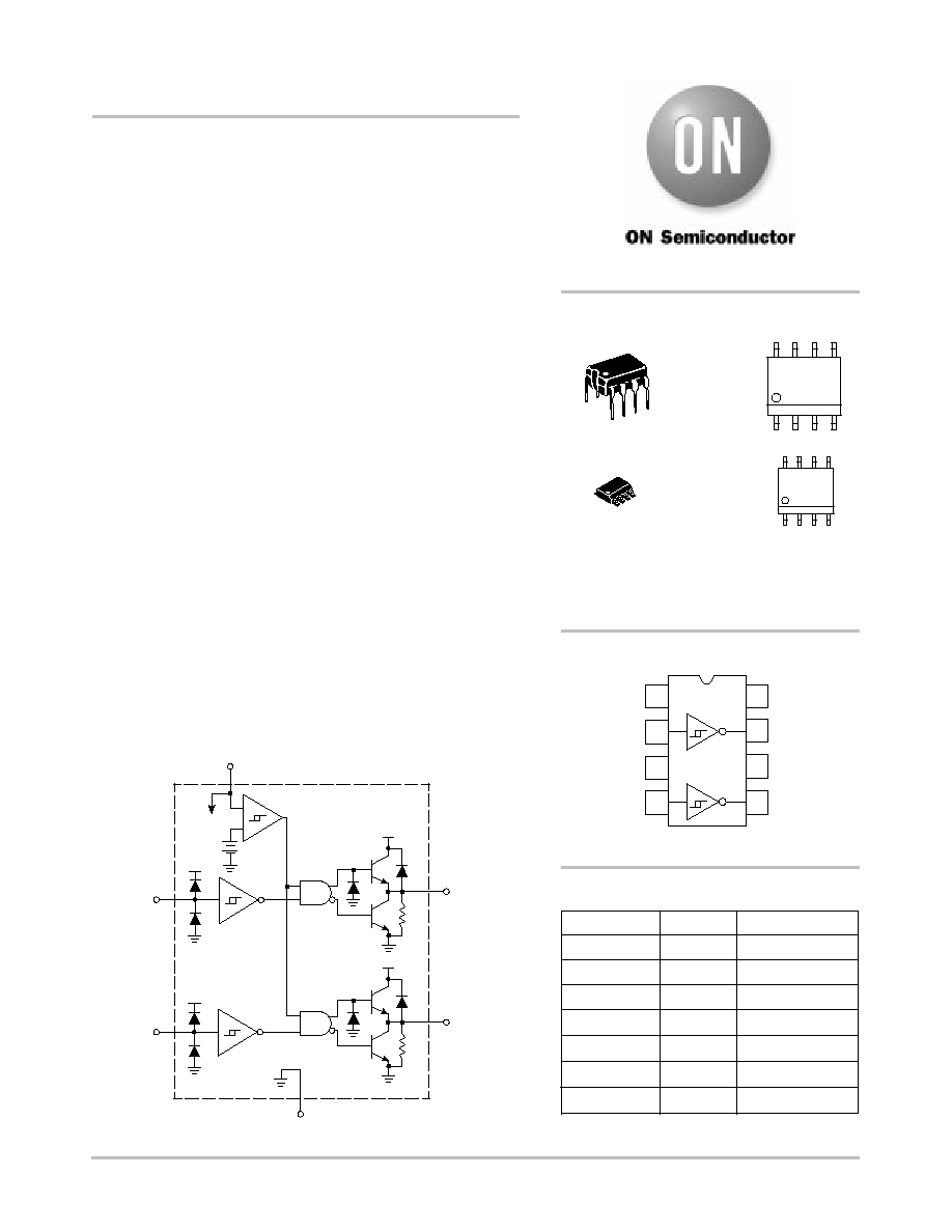
Representative Block Diagram
+
+
+
ş
VCC
6
5.7V
Logic Input A
2
Logic Input B
4
Gnd
3
100k
Drive Output A
7
Drive Output B
5
+
+
+
+
100k
Device
Package
Shipping
ORDERING INFORMATION
MC34151D
SOş8
98 Units/Rail
MC34151P
PDIPş8
MC33151D
SOş8
PDIPş8
P SUFFIX
CASE 626
1
8
http://onsemi.com
50 Units/Rail
98 Units/Rail
SOş8
D SUFFIX
CASE 751
1
8
MC33151DR2
SOş8
2500 Tape & Reel
MC34151DR2
SOş8
2500 Tape & Reel
MC33151P
PDIPş8
50 Units/Rail
MARKING
DIAGRAMS
x
= 3 or 4
A
= Assembly Location
WL, L
= Wafer Lot
YY, Y
= Year
WW, W = Work Week
PIN CONNECTIONS
1
2
3
4
5
6
7
8
N.C.
Logic Input A
Gnd
Logic Input B
N.C.
Drive Output A
VCC
Drive Output B
(Top View)
MC33151VDR2
SOş8
2500 Units/Rail
ALYW
3x151
1
8
AWL
MC3x151P
1
8
YYWW

MC34151, MC33151
http://onsemi.com
2
MAXIMUM RATINGS
Rating
Symbol
Value
Unit
Power Supply Voltage
VCC
20
V
Logic Inputs (Note 1.)
Vin
ş0.3 to VCC
V
Drive Outputs (Note 2.)
Totem Pole Sink or Source Current
Diode Clamp Current (Drive Output to VCC)
IO
IO(clamp)
1.5
1.0
A
Power Dissipation and Thermal Characteristics
D Suffix SOş8 Package Case 751
Maximum Power Dissipation @ TA = 50
░
C
Thermal Resistance, JunctionştoşAir
P Suffix 8şPin Package Case 626
Maximum Power Dissipation @ TA = 50
░
C
Thermal Resistance, JunctionştoşAir
PD
R
JA
PD
R
JA
0.56
180
1.0
100
W
░
C/W
W
░
C/W
Operating Junction Temperature
TJ
+150
░
C
Operating Ambient Temperature
MC34151
MC33151
TA
0 to +70
ş40 to +85
░
C
Storage Temperature Range
Tstg
ş65 to +150
░
C
ELECTRICAL CHARACTERISTICS
(VCC = 12 V, for typical values TA = 25
░
C, for min/max values TA is the only operating
ambient temperature range that applies [Note 3.], unless otherwise noted.)
Characteristics
Symbol
Min
Typ
Max
Unit
LOGIC INPUTS
Input Threshold Voltage ş High State Logic 1
Input Threshold Voltage
ş Low State Logic 0
VIH
VIL
2.6
ş
1.75
1.58
ş
0.8
V
Input Current ş High State (VIH = 2.6 V)
Input Current
ş Low State (VIL = 0.8 V)
IIH
IIL
ş
ş
200
20
500
100
Á
A
DRIVE OUTPUT
Output Voltage ş Low State (ISink = 10 mA)
Output Voltage ş Low State
(ISink = 50 mA)
Output Voltage ş Low State
(ISink = 400 mA)
Output Voltage
ş High State (ISource = 10 mA)
Output Voltage ş High State
(ISource = 50 mA)
Output Voltage ş High State
(ISource = 400 mA)
VOL
VOH
ş
ş
ş
10.5
10.4
9.5
0.8
1.1
1.7
11.2
11.1
10.9
1.2
1.5
2.5
ş
ş
ş
V
Output PullşDown Resistor
RPD
ş
100
ş
k
SWITCHING CHARACTERISTICS (TA = 25
░
C)
Propagation Delay (10% Input to 10% Output, CL = 1.0 nF)
Logic Input to Drive Output Rise
Logic Input to Drive Output Fall
tPLH(in/out)
tPHL(in/out)
ş
ş
35
36
100
100
ns
Drive Output Rise Time (10% to 90%) CL = 1.0 nF
Drive Output Rise Time (10% to 90%)
CL = 2.5 nF
tr
ş
ş
14
31
30
ş
ns
Drive Output Fall Time (90% to 10%) CL = 1.0 nF
Drive Output Fall Time (90% to 10%)
CL = 2.5 nF
tf
ş
ş
16
32
30
ş
ns
TOTAL DEVICE
Power Supply Current
Standby (Logic Inputs Grounded)
Operating (CL = 1.0 nF Drive Outputs 1 and 2, f = 100 kHz)
ICC
ş
ş
6.0
10.5
10
15
mA
Operating Voltage
VCC
6.5
ş
18
V
1. For optimum switching speed, the maximum input voltage should be limited to 10 V or VCC, whichever is less.
2. Maximum package power dissipation limits must be observed.
3. Tlow = 0
░
C for MC34151
Thigh = +70
░
C for MC34151
ş40
░
C for MC33151
+85
░
C for MC33151
MC34151, MC33151
http://onsemi.com
3
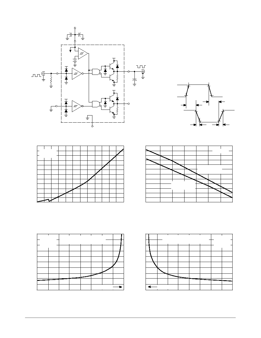
Figure 1. Switching Characteristics Test Circuit
Figure 2. Switching Waveform Definitions
Figure 3. Logic Input Current versus
Input Voltage
Figure 4. Logic Input Threshold Voltage
versus Temperature
Figure 5. Drive Output LowştoşHigh Propagation
Delay versus Logic Overdrive Voltage
Figure 6. Drive Output HighştoşLow Propagation
Delay versus Logic Input Overdrive Voltage
Vin, INPUT VOLTAGE (V)
, INPUT
CURRENT
(mA)
inI
VCC = 12 V
TA = 25
░
C
TA, AMBIENT TEMPERATURE (
░
C)
V
th
, INPUT
THRESHOLD
VOL
T
AGE (V)
VCC = 12 V
Upper Threshold
Low State Output
Lower Threshold
High State Output
Vin, INPUT OVERDRIVE VOLTAGE BELOW LOWER THRESHOLD (V)
t PLH(IN/OUT)
, DRIVE OUTPUT
PROP
AGA
TION DELA
Y
(ns)
Overdrive Voltage is with Respect
to the Logic Input Lower Threshold
Vth(lower)
VCC = 12 V
CL = 1.0 nF
TA = 25
░
C
Vin, INPUT OVERDRIVE VOLTAGE ABOVE UPPER THRESHOLD (V)
t PHL(IN/OUT)
, DRIVE OUTPUT
PROP
AGA
TION DELA
Y
(ns)
VCC = 12 V
CL = 1.0 nF
TA = 25
░
C
Vth(upper)
Overdrive Voltage is with Respect
to the Logic Input Lower Threshold
+
+
+
ş
6
5.7V
Logic Input
2
4
3
100k
Drive Output
7
5
+
+
+
+
100k
12
V
4.7
0.1
50
CL
+
5.0 V
0 V
10%
90%
tPHL
tPLH
90%
10%
tf
tr
Logic Input
tr, tf
10 ns
Drive Output
2.4
2.0
1.6
1.2
0.8
0.4
0
2.2
2.0
1.8
1.6
1.4
1.2
1.0
200
160
120
80
40
0
200
160
120
80
40
0
0
2.0
4.0
6.0
8.0
10
12
ş55
ş25
0
25
50
75
100
125
ş1.6
ş1.2
ş0.8
ş0.4
0
0
1.0
2.0
3.0
4.0
MC34151, MC33151
http://onsemi.com
4
VCC = 12 V
Vin = 5 V to 0 V
CL = 1.0 nF
TA = 25
░
C
Figure 7. Propagation Delay
Figure 8. Drive Output Clamp Voltage
versus Clamp Current
Figure 9. Drive Output Saturation Voltage
versus Load Current
Figure 10. Drive Output Saturation Voltage
versus Temperature
Figure 11. Drive Output Rise Time
Figure 12. Drive Output Fall Time
90%
10%
50 ns/DIV
90%
10%
10 ns/DIV
90%
10%
10 ns/DIV
IO, OUTPUT LOAD CURRENT (A)
V
clamp
,
OUTPUT
CLAMP
VOL
T
AGE (V)
High State Clamp
(Drive Output Driven Above VCC)
VCC
Gnd
Low State Clamp
(Drive Output Driven Below Ground)
VCC = 12 V
80
Á
s Pulsed Load
120 Hz Rate
TA = 25
░
C
IO, OUTPUT LOAD CURRENT (A)
V
sat
,
OU
T
PU
T
SA
T
URA
T
IO
N
V
O
LT
A
G
E
(V)
Source Saturation
(Load to Ground)
VCC = 12 V
80
Á
s Pulsed Load
120 Hz Rate
TA = 25
░
C
VCC
Sink Saturation
(Load to VCC)
Gnd
TA, AMBIENT TEMPERATURE (
░
C)
V
sat
, OUTPUT
SA
TURA
TION VOL
T
AGE(V)
Source Saturation
(Load to Ground)
Sink Saturation
(Load to VCC)
VCC = 12 V
Isource = 400 mA
Isink = 400 mA
VCC
Isource = 10 mA
Isink = 10 mA
Gnd
Drive Output
Logic Input
VCC = 12 V
Vin = 5 V to 0 V
CL = 1.0 nF
TA = 25
░
C
VCC = 12 V
Vin = 5 V to 0 V
CL = 1.0 nF
TA = 25
░
C
0
0.2
0.4
0.6
0.8
1.0
1.2
1.4
0
0.2
0.4
0.6
0.8
1.0
1.2
1.4
ş55
ş25
0
25
50
75
100
125
3.0
2.0
1.0
0
0
ş1.0
0
ş1.0
ş2.0
ş3.0
3.0
2.0
1.0
0
0
ş0.5
ş0.7
ş0.9
ş1.1
1.9
1.7
1.5
1.0
0.8
0.6
0
MC34151, MC33151
http://onsemi.com
5
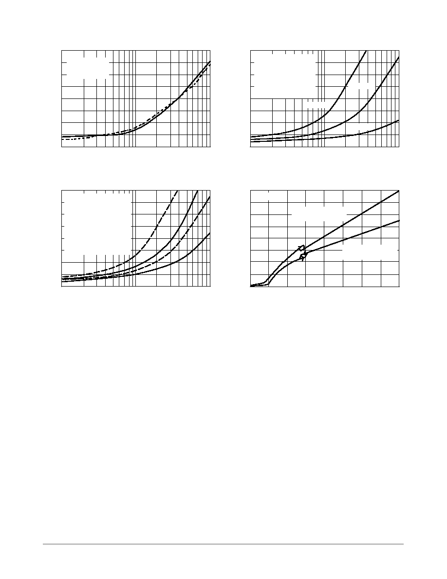
Figure 13. Drive Output Rise and Fall Time
versus Load Capacitance
Figure 14. Supply Current versus Drive Output
Load Capacitance
Figure 15. Supply Current versus Input Frequency
Figure 16. Supply Current versus Supply Voltage
CL, OUTPUT LOAD CAPACITANCE (nF)
şt
, OUTPUT
RISE-F
ALL
TIME(ns)
tf
tr
t r
VCC = 12 V
VIN = 0 V to 5.0 V
TA = 25
░
C
CL, OUTPUT LOAD CAPACITANCE (nF)
I CC
, SUPPL
Y
CURRENT
(mA)
VCC = 12 V
Both Logic Inputs Driven
0 V to 5.0 V
50% Duty Cycle
Both Drive Outputs Loaded
TA = 25
░
C
f = 500 kHz
f = 200 kHz
f = 50 kHz
I CC
, SUPPL
Y
CURRENT
(mA)
1
2
3
4
Both Logic Inputs Driven
0 V to 5.0 V,
50% Duty Cycle
Both Drive Outputs Loaded
TA = 25
░
C
1 ş VCC = 18 V, CL = 2.5 nF
2 ş VCC = 12 V, CL = 2.5 nF
3 ş VCC = 18 V, CL = 1.0 nF
4 ş VCC = 12 V, CL = 1.0 nF
f, INPUT FREQUENCY (Hz)
I CC
, SUPPL
Y
CURRENT
(mA)
VCC, SUPPLY VOLTAGE (V)
TA = 25
░
C
Logic Inputs at VCC
Low State Drive Outputs
Logic Inputs Grounded
High State Drive Outputs
f
80
60
40
20
0
80
60
40
20
0
80
60
40
20
0
8.0
6.0
4.0
2.0
0
0.1
1.0
10
0.1
1.0
10
100
1.0 M
0
4.0
8.0
12
16
10 k
APPLICATIONS INFORMATION
Description
The MC34151 is a dual inverting high speed driver
specifically designed to interface low current digital
circuitry with power MOSFETs. This device is constructed
with Schottky clamped Bipolar Analog technology which
offers a high degree of performance and ruggedness in
hostile industrial environments.
Input Stage
The Logic Inputs have 170 mV of hysteresis with the input
threshold centered at 1.67 V. The input thresholds are
insensitive to VCC making this device directly compatible
with CMOS and LSTTL logic families over its entire
operating voltage range. Input hysteresis provides fast
output switching that is independent of the input signal
transition time, preventing output oscillations as the input
thresholds are crossed. The inputs are designed to accept a
signal amplitude ranging from ground to VCC. This allows
the output of one channel to directly drive the input of a
second channel for masterşslave operation. Each input has
a 30 k
pullşdown resistor so that an unconnected open
input will cause the associated Drive Output to be in a known
high state.
Output Stage
Each totem pole Drive Output is capable of sourcing and
sinking up to 1.5 A with a typical `on' resistance of 2.4
at
1.0 A. The low `on' resistance allows high output currents
to be attained at a lower VCC than with comparative CMOS
drivers. Each output has a 100 k
pullşdown resistor to keep
the MOSFET gate low when VCC is less than 1.4 V. No over
current or thermal protection has been designed into the
device, so output shorting to VCC or ground must be
avoided.
Parasitic inductance in series with the load will cause the
driver outputs to ring above VCC during the turnşon
transition, and below ground during the turnşoff transition.
With CMOS drivers, this mode of operation can cause a
destructive output latchşup condition. The MC34151 is
immune to output latchşup. The Drive Outputs contain an
internal diode to VCC for clamping positive voltage
transients. When operating with VCC at 18 V, proper power
supply bypassing must be observed to prevent the output
ringing from exceeding the maximum 20 V device rating.
Negative output transients are clamped by the internal NPN
pullşup transistor. Since full supply voltage is applied across
MC34151, MC33151
http://onsemi.com
6
the NPN pullşup during the negative output transient, power
dissipation at high frequencies can become excessive.
Figures 19, 20, and 21 show a method of using external
Schottky diode clamps to reduce driver power dissipation.
Undervoltage Lockout
An undervoltage lockout with hysteresis prevents erratic
system operation at low supply voltages. The UVLO forces
the Drive Outputs into a low state as VCC rises from 1.4 V
to the 5.8 V upper threshold. The lower UVLO threshold is
5.3 V, yielding about 500 mV of hysteresis.
Power Dissipation
Circuit performance and long term reliability are
enhanced with reduced die temperature. Die temperature
increase is directly related to the power that the integrated
circuit must dissipate and the total thermal resistance from
the junction to ambient. The formula for calculating the
junction temperature with the package in free air is:
TJ = TA + PD (R
JA)
where:
TJ = Junction Temperature
TA = Ambient Temperature
PD = Power Dissipation
R
JA = Thermal Resistance Junction to Ambient
There are three basic components that make up total
power to be dissipated when driving a capacitive load with
respect to ground. They are:
PD = PQ + PC + PT
where:
PQ = Quiescent Power Dissipation
PC = Capacitive Load Power Dissipation
PT = Transition Power Dissipation
The quiescent power supply current depends on the
supply voltage and duty cycle as shown in Figure 16. The
device's quiescent power dissipation is:
PQ = VCC ICCL (1şD) + ICCH (D)
where:
ICCL = Supply Current with Low State Drive
Outputs
ICCH = Supply Current with High State Drive
Outputs
D = Output Duty Cycle
The capacitive load power dissipation is directly related
to the load capacitance value, frequency, and Drive Output
voltage swing. The capacitive load power dissipation per
driver is:
PC = VCC (VOH ş VOL) CL f
where:
VOH = High State Drive Output Voltage
VOL = Low State Drive Output Voltage
CL = Load Capacitance
f = frequency
When driving a MOSFET, the calculation of capacitive
load power PC is somewhat complicated by the changing
gate to source capacitance CGS as the device switches. To aid
in this calculation, power MOSFET manufacturers provide
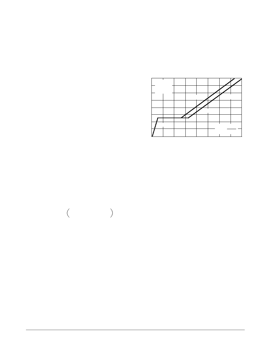
gate charge information on their data sheets. Figure 17
shows a curve of gate voltage versus gate charge for the ON
Semiconductor MTM15N50. Note that there are three
distinct slopes to the curve representing different input
capacitance values. To completely switch the MOSFET
`on', the gate must be brought to 10 V with respect to the
source. The graph shows that a gate charge Qg of 110 nC is
required when operating the MOSFET with a drain to source
voltage VDS of 400 V.
V
GS
, GA
TEşT
OşSOURCE
VOL
T
AGE
(V)
Qg, GATE CHARGE (nC)
CGS =
Qg
16
12
8.0
4.0
0
0
40
80
120
160
VDS = 100 V
VDS = 400 V
8.9 nF
2.0 nF
MTM15N50
ID = 15 A
TA = 25
░
C
Figure 17. GateşToşSource Voltage
versus Gate Charge
VGS
The capacitive load power dissipation is directly related to
the required gate charge, and operating frequency. The
capacitive load power dissipation per driver is:
PC(MOSFET) = VC Qg f
The flat region from 10 nC to 55 nC is caused by the
drainştoşgate Miller capacitance, occurring while the
MOSFET is in the linear region dissipating substantial
amounts of power. The high output current capability of the
MC34151 is able to quickly deliver the required gate charge
for fast power efficient MOSFET switching. By operating
the MC34151 at a higher VCC, additional charge can be
provided to bring the gate above 10 V. This will reduce the
`on' resistance of the MOSFET at the expense of higher
driver dissipation at a given operating frequency.
The transition power dissipation is due to extremely short
simultaneous conduction of internal circuit nodes when the
Drive Outputs change state. The transition power
dissipation per driver is approximately:
PT 9 VCC (1.08 VCC CL f ş 8 y 10ş4)
PT must be greater than zero.
Switching time characterization of the MC34151 is
performed with fixed capacitive loads. Figure 13 shows that
for small capacitance loads, the switching speed is limited
by transistor turnşon/off time and the slew rate of the
internal nodes. For large capacitance loads, the switching
speed is limited by the maximum output current capability
of the integrated circuit.

MC34151, MC33151
http://onsemi.com
7
LAYOUT CONSIDERATIONS
High frequency printed circuit layout techniques are
imperative to prevent excessive output ringing and overshoot.
Do not attempt to construct the driver circuit on
wireşwrap or plugşin prototype boards. When driving
large capacitive loads, the printed circuit board must contain
a low inductance ground plane to minimize the voltage spikes
induced by the high ground ripple currents. All high current
loops should be kept as short as possible using heavy copper
runs to provide a low impedance high frequency path. For
optimum drive performance, it is recommended that the
initial circuit design contains dual power supply bypass
capacitors connected with short leads as close to the VCC pin
and ground as the layout will permit. Suggested capacitors are
a low inductance 0.1
Á
F ceramic in parallel with a 4.7
Á
F
tantalum. Additional bypass capacitors may be required
depending upon Drive Output loading and circuit layout.
Proper printed circuit board layout is extremely
critical and cannot be over emphasized.
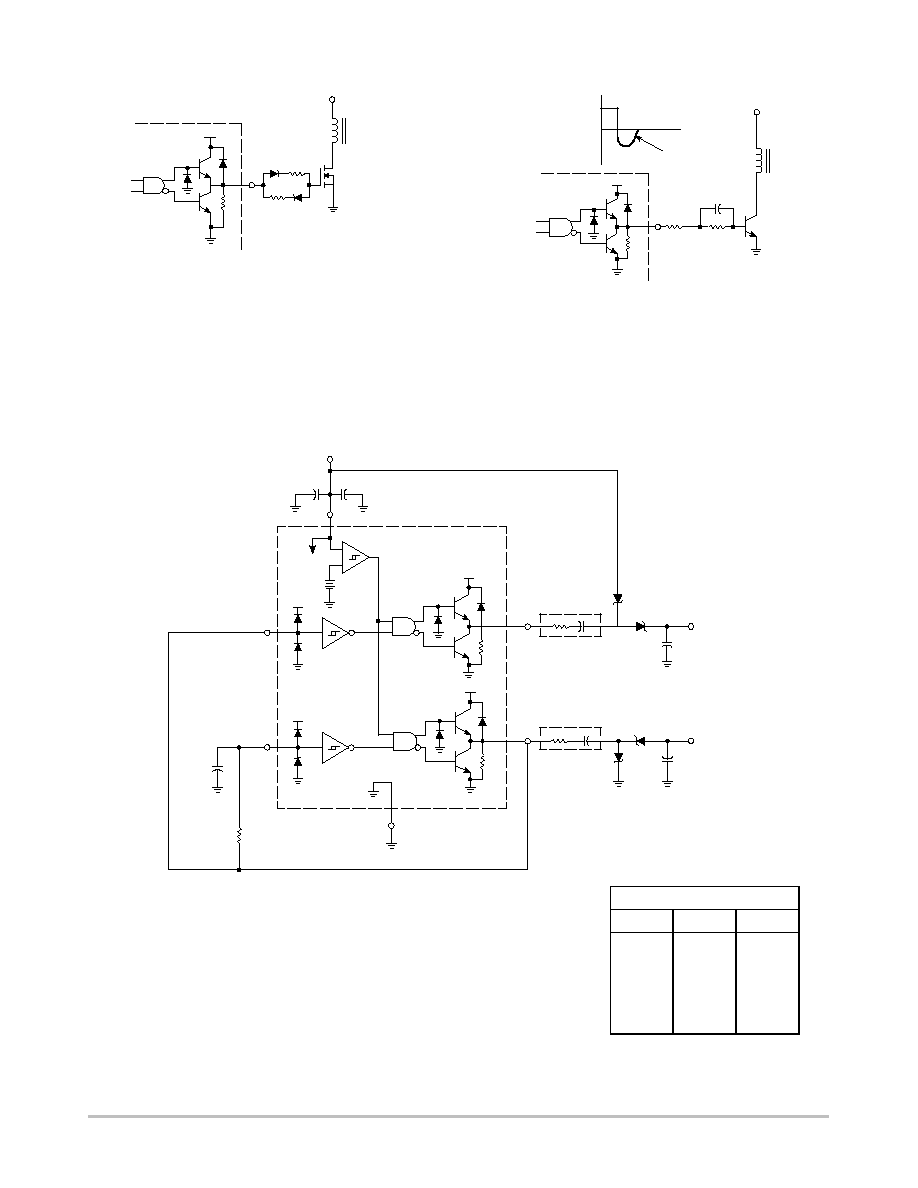
The MC34151 greatly enhances the drive capabilities of common switching
regulators and CMOS/TTL logic devices.
Figure 18. Enhanced System Performance with
Common Switching Regulators
Figure 19. MOSFET Parasitic Oscillations
Figure 20. Direct Transformer Drive
Figure 21. Isolated MOSFET Drive
Series gate resistor Rg may be needed to damp high frequency parasitic
oscillations caused by the MOSFET input capacitance and any series
wiring inductance in the gateşsource circuit. Rg will decrease the
MOSFET switching speed. Schottky diode D1 can reduce the driver's
power dissipation due to excessive ringing, by preventing the output pin
from being driven below ground.
Output Schottky diodes are recommended when driving inductive loads at
high frequencies. The diodes reduce the driver's power dissipation by
preventing the output pins from being driven above VCC and below ground.
+
ş
VCC
47
0.1
6
5.7V
TL494
or
TL594
2
4
3
100k
100k
7
5
Vin
+
+
+
+
+
+
100k
1N5819
D1
Rg
Vin
+
+
100k
100k
3
7
5
4 X
1N5819
+
+
+
+
3
100k
1N
5819
Isolation
Boundary
MC34151, MC33151
http://onsemi.com
8
Output Load Regulation
IO (mA)
+VO (V)
şVO (V)
0
27.7
ş13.3
1.0
27.4
ş12.9
10
26.4
ş11.9
20
25.5
ş11.2
30
24.6
ş10.5
50
22.6
ş9.4
Figure 22. Controlled MOSFET Drive
Figure 23. Bipolar Transistor Drive
Figure 24. Dual Charge Pump Converter
The totemşpole outputs can furnish negative base current for enhanced
transistor turnşoff, with the addition of capacitor C1.
The capacitor's equivalent series resistance limits the Drive Output Current
to 1.5 A. An additional series resistor may be required when using tantalum or
other low ESR capacitors.
In noise sensitive applications, both conducted and radiated EMI can
be reduced significantly by controlling the MOSFET's turnşon and
turnşoff times.
+
100k
Vin
Rg(on)
Rg(off)
+
IB
+
0
ş
Base Charge
Removal
100k
C1
Vin
+
ş
VCC = 15 V
4.7
0.1
6
5.7V
6.8
10
7
1N5819
2
+ VO
2.0 VCC
47
100k
100k
5
6.8 10
1N5819
4
ş VO
ş VCC
330pF
47
3
10k
+
+
+
+
+
+
+
+
+
+
+
MC34151, MC33151
http://onsemi.com
9
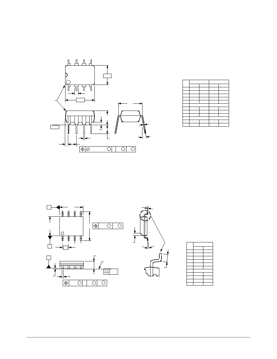
PACKAGE DIMENSIONS
PDIPş8
P SUFFIX
CASE 626ş05
ISSUE K
NOTES:
1. DIMENSION L TO CENTER OF LEAD WHEN
FORMED PARALLEL.
2. PACKAGE CONTOUR OPTIONAL (ROUND OR
SQUARE CORNERS).
3. DIMENSIONING AND TOLERANCING PER ANSI
Y14.5M, 1982.
1
4
5
8
F
NOTE 2
şAş
şBş
şTş
SEATING
PLANE
H
J
G
D
K
N
C
L
M
M
A
M
0.13 (0.005)
B
M
T
DIM
MIN
MAX
MIN
MAX
INCHES
MILLIMETERS
A
9.40
10.16
0.370
0.400
B
6.10
6.60
0.240
0.260
C
3.94
4.45
0.155
0.175
D
0.38
0.51
0.015
0.020
F
1.02
1.78
0.040
0.070
G
2.54 BSC
0.100 BSC
H
0.76
1.27
0.030
0.050
J
0.20
0.30
0.008
0.012
K
2.92
3.43
0.115
0.135
L
7.62 BSC
0.300 BSC
M
şşş
10
şşş
10
N
0.76
1.01
0.030
0.040
_
_
SOş8
D SUFFIX
CASE 751ş06
ISSUE T
SEATING
PLANE
1
4
5
8
A
0.25
M
C B
S
S
0.25
M
B
M
h
q
C
X 45
_
L
DIM
MIN
MAX
MILLIMETERS
A
1.35
1.75
A1
0.10
0.25
B
0.35
0.49
C
0.19
0.25
D
4.80
5.00
E
1.27 BSC
e
3.80
4.00
H
5.80
6.20
h
0
7
L
0.40
1.25
q
0.25
0.50
_
_
NOTES:
1. DIMENSIONING AND TOLERANCING PER ASME
Y14.5M, 1994.
2. DIMENSIONS ARE IN MILLIMETER.
3. DIMENSION D AND E DO NOT INCLUDE MOLD
PROTRUSION.
4. MAXIMUM MOLD PROTRUSION 0.15 PER SIDE.
5. DIMENSION B DOES NOT INCLUDE DAMBAR
PROTRUSION. ALLOWABLE DAMBAR
PROTRUSION SHALL BE 0.127 TOTAL IN EXCESS
OF THE B DIMENSION AT MAXIMUM MATERIAL
CONDITION.
D
E
H
A
B
e
B
A1
C
A
0.10

MC34151, MC33151
http://onsemi.com
10
Notes

MC34151, MC33151
http://onsemi.com
11
Notes

MC34151, MC33151
http://onsemi.com
12
ON Semiconductor and are trademarks of Semiconductor Components Industries, LLC (SCILLC). SCILLC reserves the right to make changes
without further notice to any products herein. SCILLC makes no warranty, representation or guarantee regarding the suitability of its products for any particular
purpose, nor does SCILLC assume any liability arising out of the application or use of any product or circuit, and specifically disclaims any and all liability,
including without limitation special, consequential or incidental damages. "Typical" parameters which may be provided in SCILLC data sheets and/or
specifications can and do vary in different applications and actual performance may vary over time. All operating parameters, including "Typicals" must be
validated for each customer application by customer's technical experts. SCILLC does not convey any license under its patent rights nor the rights of others.
SCILLC products are not designed, intended, or authorized for use as components in systems intended for surgical implant into the body, or other applications
intended to support or sustain life, or for any other application in which the failure of the SCILLC product could create a situation where personal injury or
death may occur. Should Buyer purchase or use SCILLC products for any such unintended or unauthorized application, Buyer shall indemnify and hold
SCILLC and its officers, employees, subsidiaries, affiliates, and distributors harmless against all claims, costs, damages, and expenses, and reasonable
attorney fees arising out of, directly or indirectly, any claim of personal injury or death associated with such unintended or unauthorized use, even if such claim
alleges that SCILLC was negligent regarding the design or manufacture of the part. SCILLC is an Equal Opportunity/Affirmative Action Employer.
PUBLICATION ORDERING INFORMATION
CENTRAL/SOUTH AMERICA:
Spanish Phone: 303ş308ş7143 (MonşFri 8:00am to 5:00pm MST)
Email: ONlitşspanish@hibbertco.com
ASIA/PACIFIC: LDC for ON Semiconductor ş Asia Support
Phone: 303ş675ş2121 (TueşFri 9:00am to 1:00pm, Hong Kong Time)
Toll Free from Hong Kong & Singapore:
001ş800ş4422ş3781
Email: ONlitşasia@hibbertco.com
JAPAN: ON Semiconductor, Japan Customer Focus Center
4ş32ş1 NishişGotanda, Shinagawaşku, Tokyo, Japan 141ş8549
Phone: 81ş3ş5740ş2745
Email: r14525@onsemi.com
ON Semiconductor Website: http://onsemi.com
For additional information, please contact your local
Sales Representative.
MC34151/D
NORTH AMERICA Literature Fulfillment:
Literature Distribution Center for ON Semiconductor
P.O. Box 5163, Denver, Colorado 80217 USA
Phone: 303ş675ş2175 or 800ş344ş3860 Toll Free USA/Canada
Fax: 303ş675ş2176 or 800ş344ş3867 Toll Free USA/Canada
Email: ONlit@hibbertco.com
Fax Response Line: 303ş675ş2167 or 800ş344ş3810 Toll Free USA/Canada
N. American Technical Support: 800ş282ş9855 Toll Free USA/Canada
EUROPE: LDC for ON Semiconductor ş European Support
German Phone: (+1) 303ş308ş7140 (MşF 1:00pm to 5:00pm Munich Time)
Email: ONlitşgerman@hibbertco.com
French Phone: (+1) 303ş308ş7141 (MşF 1:00pm to 5:00pm Toulouse Time)
Email: ONlitşfrench@hibbertco.com
English Phone: (+1) 303ş308ş7142 (MşF 12:00pm to 5:00pm UK Time)
Email: ONlit@hibbertco.com
EUROPEAN TOLLşFREE ACCESS*: 00ş800ş4422ş3781
*Available from Germany, France, Italy, England, Ireland