MOTOROLA
SEMICONDUCTOR TECHNICAL DATA
2Ù77
REV 5
ˋ
Motorola, Inc. 1996
3/93
Quad TTL/NMOS to PECL*
Translator
The MC10H351 is a quad translator for interfacing data between a
saturated logic section and the PECL section of digital systems when only
a +5.0 Vdc power supply is available. The MC10H351 has TTL/NMOS
compatible inputs and PECL complementary openÙemitter outputs that
allow use as an inverting/nonÙinverting translator or as a differential line
driver. When the common strobe input is at a low logic level, it forces all
true outputs to the PECL low logic state (
+3.2 V) and all inverting
outputs to the PECL high logic state (
+4.1 V).
The MC10H351 can also be used with the MC10H350 to transmit and
receive TTL/NMOS information differentially via balanced twisted pair
lines.
ñ
Single +5.0 Power Supply
ñ
All VCC Pins Isolated On Chip
ñ
Differentially Drive Balanced Lines
ñ
tpd = 1.3 nsec Typical
MAXIMUM RATINGS
Characteristic
Symbol
Rating
Unit
Power Supply
VCC
0 to +7.0
Vdc
Input Voltage (VCC = 5.0 V)
VI
0 to VCC
Vdc
Output Current -- Continuous
-- Surge
Iout
50
100
mA
Operating Temperature Range
TA
0 to +75
¯
C
Storage Temperature Range -- Plastic
-- Ceramic
Tstg
Ù55 to +150
Ù55 to +165
¯
C
ELECTRICAL CHARACTERISTICS (VCC = VCC1 = VCC2 = 5.0 V
Ý
5.0%)
0
¯
25
¯
75
¯
Characteristic
Symbol
Min
Max
Min
Max
Min
Max
Unit
Power Supply
C
t
ECL
--
50
--
45
--
50
mA
pp y
Current
TTL
--
20
--
15
--
20
mA
Reverse Current
Pins 7, 8, 12, 14
Pin 9
IR
IINH
--
--
25
100
--
--
20
80
--
--
25
100
ç
A
Forward Current
Pins 7, 8, 12, 14
Pin 9
IF
IINL
--
--
Ù0.8
Ù3.2
--
--
Ù0.6
Ù2.4
--
--
Ù0.8
Ù3.2
mA
Input Breakdown
Voltage
V(BR)in
5.5
--
5.5
--
5.5
--
Vdc
Input Clamp Voltage
(Iin = Ù18 mA)
VI
--
Ù1.5
--
Ù1.5
--
Ù1.5
Vdc
High Output
Voltage (1)
VOH
3.98
4.16
4.02
4.19
4.08
4.27
Vdc
Low Output
Voltage (1)
VOL
3.05
3.37
3.05
3.37
3.05
3.37
Vdc
High Input Voltage
VIH
2.0
--
2.0
--
2.0
--
Vdc
Low Input Voltage
VIL
--
0.8
--
0.8
--
0.8
Vdc
(1) With VCC at 5.0 V. VOH/VOL change 1:1 with VCC.
*Positive Emitter Coupled Logic
MC10H351
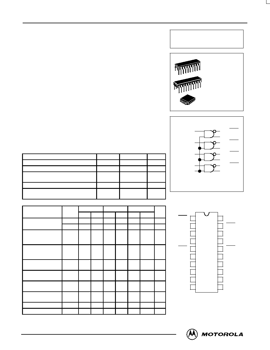
LOGIC DIAGRAM
DIP
PIN ASSIGNMENT
B OUT
B OUT
N.C.
A OUT
A OUT
VCC
B IN
A IN
ECL VCC
C OUT
C OUT
D OUT
D OUT
VCC 2
C IN
N.C.
20
19
18
17
16
15
14
13
1
2
3
4
5
6
7
8
COMMON
STROBE
GND
D IN
TTL VCC
12
11
9
10
14
19
18
12
16
17
8
5
4
7
1
2
9
B IN
A IN
COMMON
STROBE
D IN
C IN
B OUT
B OUT
A OUT
A OUT
D OUT
D OUT
C OUT
C OUT
VCC (+5.0 VDC) = PINS 6, 11, 15, 20
GND = PIN 10
L SUFFIX
CERAMIC PACKAGE
CASE 732Ù03
P SUFFIX
PLASTIC PACKAGE
CASE 738Ù03
FN SUFFIX
PLCC
CASE 775Ù02
Pin assignment is for DualÙinÙLine Package.
For PLCC pin assignment, see the Pin Conversion
Tables on page 6Ù36 of the Motorola MECL Data
Book (DL122/D).
MC10H351
MOTOROLA
MECL Data
DL122 -- Rev 6
2Ù78
AC PARAMETERS
0
¯
25
¯
75
¯
Characteristic
Symbol
Min
Max
Min
Max
Min
Max
Unit
Propagation Delay (1)
tpd
0.4
2.2
0.4
2.2
0.4
2.1
ns
Rise Time (20% to 80%)
tr
0.4
1.9
0.4
2.0
0.4
2.1
ns
Fall Time (80% to 20%)
tf
0.4
1.9
0.4
2.0
0.4
2.1
ns
Maximum Operating Frequency
fmax
150
--
150
--
150
--
MHz
(1) Propagation delay is measured on this circuit from +1.5 volts on the input waveform to the 50% point on the output waveform.
NOTE:
Each MECL 10H series circuit has been designed to meet the dc specifications shown in the test table, after thermal equilibrium has been established. The
circuit is in a test socket or mounted on a printed circuit board and transverse air flow greater than 500 lfpm is maintained. Outputs are terminated through
a 50Ùohm resistor to VCC Ù2.0 Vdc.

MC10H351
2Ù79
MOTOROLA
MECL Data
DL122 -- Rev 6
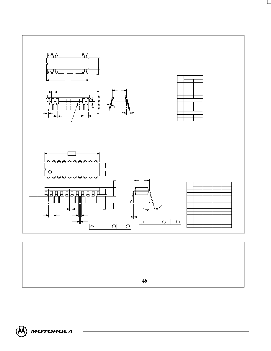
OUTLINE DIMENSIONS
FN SUFFIX
PLASTIC PLCC PACKAGE
CASE 775Ù02
ISSUE C
NOTES:
1. DATUMS ÙLÙ, ÙMÙ, AND ÙNÙ DETERMINED
WHERE TOP OF LEAD SHOULDER EXITS PLASTIC
BODY AT MOLD PARTING LINE.
2. DIMENSION G1, TRUE POSITION TO BE
MEASURED AT DATUM ÙTÙ, SEATING PLANE.
3. DIMENSIONS R AND U DO NOT INCLUDE MOLD
FLASH. ALLOWABLE MOLD FLASH IS 0.010 (0.250)
PER SIDE.
4. DIMENSIONING AND TOLERANCING PER ANSI
Y14.5M, 1982.
5. CONTROLLING DIMENSION: INCH.
6. THE PACKAGE TOP MAY BE SMALLER THAN THE
PACKAGE BOTTOM BY UP TO 0.012 (0.300).
DIMENSIONS R AND U ARE DETERMINED AT THE
OUTERMOST EXTREMES OF THE PLASTIC BODY
EXCLUSIVE OF MOLD FLASH, TIE BAR BURRS,
GATE BURRS AND INTERLEAD FLASH, BUT
INCLUDING ANY MISMATCH BETWEEN THE TOP
AND BOTTOM OF THE PLASTIC BODY.
7. DIMENSION H DOES NOT INCLUDE DAMBAR
PROTRUSION OR INTRUSION. THE DAMBAR
PROTRUSION(S) SHALL NOT CAUSE THE H
DIMENSION TO BE GREATER THAN 0.037 (0.940).
THE DAMBAR INTRUSION(S) SHALL NOT CAUSE
THE H DIMENSION TO BE SMALLER THAN 0.025
(0.635).
ÙMÙ
ÙNÙ
ÙLÙ
Y BRK
W
V
D
D
S
LÙM
M
0.007 (0.180)
N
S
T
S
LÙM
M
0.007 (0.180)
N
S
T
S
LÙM
S
0.010 (0.250)
N
S
T
X
G1
B
U
Z
VIEW DÙD
20
1
S
LÙM
M
0.007 (0.180)
N
S
T
S
LÙM
M
0.007 (0.180)
N
S
T
S
LÙM
S
0.010 (0.250)
N
S
T
C
G
VIEW S
E
J
R
Z
A
0.004 (0.100)
ÙTÙ
SEATING
PLANE
S
LÙM
M
0.007 (0.180)
N
S
T
S
LÙM
M
0.007 (0.180)
N
S
T
H
VIEW S
K
K1
F
G1
DIM
MIN
MAX
MIN
MAX
MILLIMETERS
INCHES
A
0.385
0.395
9.78
10.03
B
0.385
0.395
9.78
10.03
C
0.165
0.180
4.20
4.57
E
0.090
0.110
2.29
2.79
F
0.013
0.019
0.33
0.48
G
0.050 BSC
1.27 BSC
H
0.026
0.032
0.66
0.81
J
0.020
ÙÙÙ
0.51
ÙÙÙ
K
0.025
ÙÙÙ
0.64
ÙÙÙ
R
0.350
0.356
8.89
9.04
U
0.350
0.356
8.89
9.04
V
0.042
0.048
1.07
1.21
W
0.042
0.048
1.07
1.21
X
0.042
0.056
1.07
1.42
Y
ÙÙÙ
0.020
ÙÙÙ
0.50
Z
2
10
2
10
G1
0.310
0.330
7.88
8.38
K1
0.040
ÙÙÙ
1.02
ÙÙÙ
_
_
_
_
MC10H351
MOTOROLA
MECL Data
DL122 -- Rev 6
2Ù80
OUTLINE DIMENSIONS
P SUFFIX
PLASTIC DIP PACKAGE
CASE 738Ù03
ISSUE E
L SUFFIX
CERAMIC DIP PACKAGE
CASE 732Ù03
ISSUE E
NOTES:
1. LEADS WITHIN 0.010 DIAMETER, TRUE
POSITION AT SEATING PLANE, AT MAXIMUM
MATERIAL CONDITION.
2. DIMENSION L TO CENTER OF LEADS WHEN
FORMED PARALLEL.
3. DIMENSIONS A AND B INCLUDE MENISCUS.
DIM
MIN
MAX
INCHES
A
0.940
0.990
B
0.260
0.295
C
0.150
0.200
D
0.015
0.022
F
0.055
0.065
G
0.100 BSC
H
0.020
0.050
J
0.008
0.012
K
0.125
0.160
L
0.300 BSC
M
0
15
N
0.010
0.040
_
_
A
20
1
10
11
B
F
C
SEATING
PLANE
D
H
G
K
N
J
M
L
NOTES:
1. DIMENSIONING AND TOLERANCING PER ANSI
Y14.5M, 1982.
2. CONTROLLING DIMENSION: INCH.
3. DIMENSION L TO CENTER OF LEAD WHEN
FORMED PARALLEL.
4. DIMENSION B DOES NOT INCLUDE MOLD
FLASH.
M
L
J
20 PL
M
B
M
0.25 (0.010)
T
DIM
MIN
MAX
MIN
MAX
MILLIMETERS
INCHES
A
25.66
27.17
1.010
1.070
B
6.10
6.60
0.240
0.260
C
3.81
4.57
0.150
0.180
D
0.39
0.55
0.015
0.022
G
2.54 BSC
0.100 BSC
J
0.21
0.38
0.008
0.015
K
2.80
3.55
0.110
0.140
L
7.62 BSC
0.300 BSC
M
0
15
0
15
N
0.51
1.01
0.020
0.040
_
_
_
_
E
1.27
1.77
0.050
0.070
1
11
10
20
ÙAÙ
SEATING
PLANE
K
N
F
G
D
20 PL
ÙTÙ
M
A
M
0.25 (0.010)
T
E
B
C
F
1.27 BSC
0.050 BSC
Motorola reserves the right to make changes without further notice to any products herein. Motorola makes no warranty, representation or guarantee regarding
the suitability of its products for any particular purpose, nor does Motorola assume any liability arising out of the application or use of any product or circuit, and
specifically disclaims any and all liability, including without limitation consequential or incidental damages. "Typical" parameters which may be provided in Motorola
data sheets and/or specifications can and do vary in different applications and actual performance may vary over time. All operating parameters, including "Typicals"
must be validated for each customer application by customer's technical experts. Motorola does not convey any license under its patent rights nor the rights of
others. Motorola products are not designed, intended, or authorized for use as components in systems intended for surgical implant into the body, or other
applications intended to support or sustain life, or for any other application in which the failure of the Motorola product could create a situation where personal injury
or death may occur. Should Buyer purchase or use Motorola products for any such unintended or unauthorized application, Buyer shall indemnify and hold Motorola
and its officers, employees, subsidiaries, affiliates, and distributors harmless against all claims, costs, damages, and expenses, and reasonable attorney fees
arising out of, directly or indirectly, any claim of personal injury or death associated with such unintended or unauthorized use, even if such claim alleges that
Motorola was negligent regarding the design or manufacture of the part. Motorola and are registered trademarks of Motorola, Inc. Motorola, Inc. is an Equal
Opportunity/Affirmative Action Employer.
How to reach us:
USA/EUROPE/Locations Not Listed: Motorola Literature Distribution;
JAPAN: Nippon Motorola Ltd.; TatsumiÙSPDÙJLDC, 6F SeibuÙButsuryuÙCenter,
P.O. Box 20912; Phoenix, Arizona 85036. 1Ù800Ù441Ù2447 or 602Ù303Ù5454
3Ù14Ù2 Tatsumi KotoÙKu, Tokyo 135, Japan. 03Ù81Ù3521Ù8315
MFAX: RMFAX0@email.sps.mot.com Ù TOUCHTONE 602Ù244Ù6609
ASIA/PACIFIC: Motorola Semiconductors H.K. Ltd.; 8B Tai Ping Industrial Park,
INTERNET: http://DesignÙNET.com
51 Ting Kok Road, Tai Po, N.T., Hong Kong. 852Ù26629298
MC10H351/D
*MC10H351/D*