©
Semiconductor Components Industries, LLC, 2004
January, 2004 - Rev. 12
1
Publication Order Number:
MC10EP56/D
MC10EP56, MC100EP56
3.3V / 5V ECL Dual
Differential 2:1 Multiplexer
The MC10/100EP56 is a dual, fully differential 2:1 multiplexer. The
differential data path makes the device ideal for multiplexing low
skew clock or other skew sensitive signals. Multiple V
BB
pins are
provided.
The V
BB
pin, an internally generated voltage supply, is available to
this device only. For single-ended input conditions, the unused
differential input is connected to V
BB
as a switching reference voltage.
V
BB
may also rebias AC coupled inputs. When used, decouple V
BB
and V
CC
via a 0.01
mF capacitor and limit current sourcing or sinking
to 0.5 mA. When not used, V
BB
should be left open.
The device features both individual and common select inputs to
address both data path and random logic applications.
The 100 Series contains temperature compensation.
·
360 ps Typical Propagation Delays
·
Maximum Frequency > 3 GHz Typical
·
PECL Mode Operating Range: V
CC
= 3.0 V to 5.5 V
with V
EE
= 0 V
·
NECL Mode Operating Range: V
CC
= 0 V
with V
EE
= -3.0 V to -5.5 V
·
Open Input Default State
·
Safety Clamp on Inputs
·
Separate and Common Select
·
Q Output Will Default LOW with Inputs Open or at V
EE
·
V
BB
Outputs
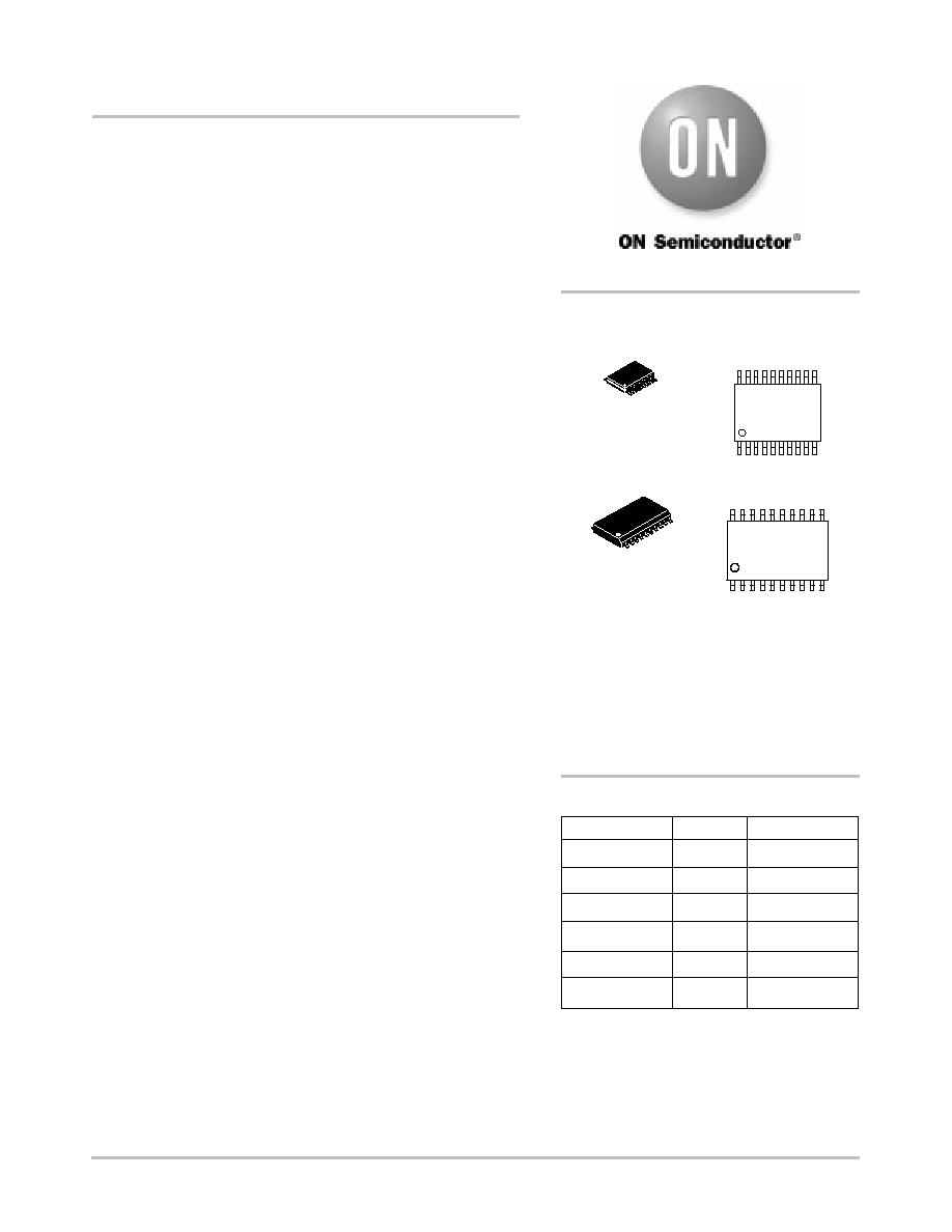
Device
Package
Shipping
ORDERING INFORMATION
MC10EP56DT
TSSOP-20
75 Units/Rail
MC10EP56DTR2
TSSOP-20 2500 Tape & Reel
TSSOP-20
DT SUFFIX
CASE 948E
MARKING
DIAGRAMS*
xxx
= MC10 or 100
A
= Assembly Location
L, WL
= Wafer Lot
Y, YY
= Year
W, WW = Work Week
*For additional information, see Application Note
AND8002/D
MC100EP56DT
TSSOP-20
75 Units/Rail
MC100EP56DTR2
TSSOP-20 2500 Tape & Reel
SO-20
DW SUFFIX
CASE 751D
1
20
MC100EP56
AWLYYWW
MC100EP56DW
SO-20
38 Units/Rail
MC100EP56DWR2
SO-20
1000 Tape & Reel
1
20
xxxx
EP56
ALYW
1
20
20
1
http://onsemi.com
For information on tape and reel specifications,
including part orientation and tape sizes, please
refer to our Tape and Reel Packaging Specification
Brochure, BRD8011/D.

MC10EP56, MC100EP56
http://onsemi.com
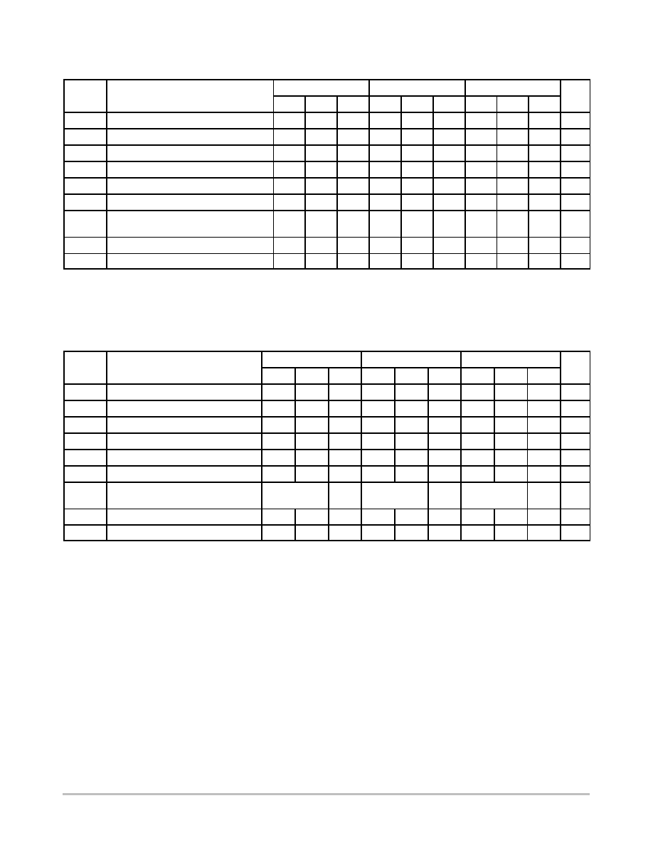
2
D0b
D0b
D1a
V
BBO
17
18
16
15
14
13
12
4
3
5
6
7
8
9
Q0
11
10
SEL0
SEL1
V
CC
Q1
Q1
V
EE
D0a
19
20
2
1
V
CC
Q0
D1a
D0a
COM_SEL
V
BB1
D1b
D1b
1
0
1
0
PIN DESCRIPTION
PIN
D0a* - D1a*
D0a* - D1a*
ECL Input Data a Invert
FUNCTION
ECL Input Data a
D0b* - D1b*
D0b* - D1b*
ECL Input Data b Invert
ECL Input Data b
SEL0* - SEL1*
COM_SEL*
ECL Common Select Input
ECL Indiv. Select Input
V
BB0
, V
BB1
Q0 - Q1
ECL True Outputs
Output Reference Voltage
Q0 - Q1
ECL Inverted Outputs
V
CC
Positive Supply
V
EE
Negative Supply
SEL0
X
L
L
H
H
TRUTH TABLE
Q0,
Q0
a
b
b
a
a
SEL1
X
L
H
H
L
COM_SEL
H
L
L
L
L
Q1,
Q1
a
b
a
a
b
Warning: All V
CC
and V
EE
pins must be externally connected
to Power Supply to guarantee proper operation.
Figure 1. 20-Lead Package (Top View) and Logic Diagram
* Pins will default LOW when left open.
ATTRIBUTES
Characteristics
Value
Internal Input Pulldown Resistor
75 k
W
Internal Input Pullup Resistor
N/A
ESD Protection
Human Body Model
Machine Model
Charged Device Model
> 2 kV
> 150 V
> 2 kV
Moisture Sensitivity, Indefinite Time Out of Drypack (Note 1)
Level 1
Flammability Rating
Oxygen Index: 28 to 34
UL 94 V-0 @ 0.125 in
Transistor Count
140 Devices
Meets or exceeds JEDEC Spec EIA/JESD78 IC Latchup Test
1. For additional information, see Application Note AND8003/D.

MC10EP56, MC100EP56
http://onsemi.com
3
MAXIMUM RATINGS
(Note 2)
Symbol
Parameter
Condition 1
Condition 2
Rating
Units
V
CC
PECL Mode Power Supply
V
EE
= 0 V
6
V
V
EE
NECL Mode Power Supply
V
CC
= 0 V
-6
V
V
I
PECL Mode Input Voltage
V
EE
= 0 V
V
I
V
CC
6
V
V
I
PECL Mode In ut Voltage
NECL Mode Input Voltage
V
EE
0 V
V
CC
= 0 V
V
I
V
CC
V
I
V
EE
6
-6
V
V
I
out
Output Current
Continuous
Surge
50
100
mA
mA
I
BB
V
BB
Sink/Source
±
0.5
mA
TA
Operating Temperature Range
-40 to +85
°
C
T
stg
Storage Temperature Range
-65 to +150
°
C
q
JA
Thermal Resistance (Junction-to-Ambient)
0 LFPM
500 LFPM
20 TSSOP
20 TSSOP
140
100
°
C/W
°
C/W
q
JC
Thermal Resistance (Junction-to-Case)
std bd
20 TSSOP
23 to 41
°
C/W
q
JA
Thermal Resistance (Junction-to-Ambient)
0 LFPM
500 LFPM
20 SOIC
20 SOIC
90
60
°
C/W
°
C/W
q
JC
Thermal Resistance (Junction-to-Case)
std bd
20 SOIC
33 to 35
°
C/W
T
sol
Wave Solder
<2 to 3 sec @ 248
°
C
265
°
C
2. Maximum Ratings are those values beyond which device damage may occur.
10EP DC CHARACTERISTICS, PECL
V
CC
= 3.3 V, V
EE
= 0 V (Note 3)
-40
°
C
25
°
C
85
°
C
Symbol
Characteristic
Min
Typ
Max
Min
Typ
Max
Min
Typ
Max
Unit
I
EE
Power Supply Current
50
61
75
50
63
75
55
65
78
mA
V
OH
Output HIGH Voltage (Note 4)
2165
2290
2415
2230
2355
2480
2290
2415
2540
mV
V
OL
Output LOW Voltage (Note 4)
1365
1490
1615
1430
1555
1680
1490
1615
1740
mV
V
IH
Input HIGH Voltage (Single-Ended)
2090
2415
2155
2480
2215
2540
mV
V
IL
Input LOW Voltage (Single-Ended)
1365
1690
1460
1755
1490
1815
mV
V
BB
Output Voltage Reference
1790
1890
1990
1855
1955
2055
1915
2015
2115
mV
V
IHCMR
Input HIGH Voltage Common Mode
Range (Differential) (Note 5)
2.0
3.3
2.0
3.3
2.0
3.3
V
I
IH
Input HIGH Current
150
150
150
m
A
I
IL
Input LOW Current
0.5
0.5
0.5
m
A
NOTE: EP circuits are designed to meet the DC specifications shown in the above table after thermal equilibrium has been established. The
circuit is in a test socket or mounted on a printed circuit board and transverse airflow greater than 500 lfpm is maintained.
3. Input and output parameters vary 1:1 with V
CC
. V
EE
can vary +0.3 V to -2.2 V.
4. All loading with 50
W
to V
CC
-2.0 volts.
5. V
IHCMR
min varies 1:1 with V
EE
, V
IHCMR
max varies 1:1 with V
CC
. The V
IHCMR
range is referenced to the most positive side of the differential
input signal.
MC10EP56, MC100EP56
http://onsemi.com
4
10EP DC CHARACTERISTICS, PECL
V
CC
= 5.0 V, V
EE
= 0 V (Note 6)
-40
°
C
25
°
C
85
°
C
Symbol
Characteristic
Min
Typ
Max
Min
Typ
Max
Min
Typ
Max
Unit
I
EE
Power Supply Current
50
61
75
50
63
75
55
65
78
mA
V
OH
Output HIGH Voltage (Note 7)
3865
3990
4115
3930
4055
4180
3990
4115
4240
mV
V
OL
Output LOW Voltage (Note 7)
3065
3190
3315
3130
3255
3380
3190
3315
3440
mV
V
IH
Input HIGH Voltage (Single-Ended)
3790
4115
3855
4180
3915
4240
mV
V
IL
Input LOW Voltage (Single-Ended)
3065
3390
3130
3455
3190
3515
mV
V
BB
Output Voltage Reference
3490
3590
3690
3555
3655
3755
3615
3715
3815
mV
V
IHCMR
Input HIGH Voltage Common Mode
Range (Differential) (Note 8)
2.0
5.0
2.0
5.0
2.0
5.0
V
I
IH
Input HIGH Current
150
150
150
m
A
I
IL
Input LOW Current
0.5
0.5
0.5
m
A
NOTE: EP circuits are designed to meet the DC specifications shown in the above table after thermal equilibrium has been established. The
circuit is in a test socket or mounted on a printed circuit board and transverse airflow greater than 500 lfpm is maintained.
6. Input and output parameters vary 1:1 with V
CC
. V
EE
can vary +2.0 V to -0.5 V.
7. All loading with 50
W
to V
CC
-2.0 volts.
8. V
IHCMR
min varies 1:1 with V
EE
, V
IHCMR
max varies 1:1 with V
CC
. The V
IHCMR
range is referenced to the most positive side of the differential
input signal.
10EP DC CHARACTERISTICS, NECL
V
CC
= 0 V, V
EE
= -5.5 V to -3.0 V (Note 9)
-40
°
C
25
°
C
85
°
C
Symbol
Characteristic
Min
Typ
Max
Min
Typ
Max
Min
Typ
Max
Unit
I
EE
Power Supply Current
50
61
75
50
63
75
55
65
78
mA
V
OH
Output HIGH Voltage (Note 10)
-1135
-1010
-885
-1070
-945
-820
-1010
-885
-760
mV
V
OL
Output LOW Voltage (Note 10)
-1935
-1810
-1685
-1870
-1745
-1620
-1810
-1685
-1560
mV
V
IH
Input HIGH Voltage (Single-Ended)
-1210
-885
-1145
-820
-1085
-760
mV
V
IL
Input LOW Voltage (Single-Ended)
-1935
-1610
-1870
-1545
-1810
-1485
mV
V
BB
Output Voltage Reference
-1510
-1410
-1310
-1445
-1345
-1245
-1385
-1285
-1185
mV
V
IHCMR
Input HIGH Voltage Common Mode
Range (Differential) (Note 11)
V
EE
+2.0
0.0
V
EE
+2.0
0.0
V
EE
+2.0
0.0
V
I
IH
Input HIGH Current
150
150
150
m
A
I
IL
Input LOW Current
0.5
0.5
0.5
m
A
NOTE: EP circuits are designed to meet the DC specifications shown in the above table after thermal equilibrium has been established. The
circuit is in a test socket or mounted on a printed circuit board and transverse airflow greater than 500 lfpm is maintained.
9. Input and output parameters vary 1:1 with V
CC
.
10. All loading with 50
W
to V
CC
-2.0 volts.
11. V
IHCMR
min varies 1:1 with V
EE
, V
IHCMR
max varies 1:1 with V
CC
. The V
IHCMR
range is referenced to the most positive side of the differential
input signal.

MC10EP56, MC100EP56
http://onsemi.com
5
100EP DC CHARACTERISTICS, PECL
V
CC
= 3.3 V, V
EE
= 0 V (Note 12)
-40
°
C
25
°
C
85
°
C
Symbol
Characteristic
Min
Typ
Max
Min
Typ
Max
Min
Typ
Max
Unit
I
EE
Power Supply Current
50
61
75
50
63
77
55
66
80
mA
V
OH
Output HIGH Voltage (Note 13)
2155
2280
2405
2155
2280
2405
2155
2280
2405
mV
V
OL
Output LOW Voltage (Note 13)
1355
1480
1605
1355
1480
1605
1355
1480
1605
mV
V
IH
Input HIGH Voltage (Single-Ended)
2075
2420
2075
2420
2075
2420
mV
V
IL
Input LOW Voltage (Single-Ended)
1355
1675
1355
1675
1355
1675
mV
V
BB
Output Voltage Reference
1775
1875
1975
1775
1875
1975
1775
1875
1975
mV
V
IHCMR
Input HIGH Voltage Common Mode
Range (Differential) (Note 14)
2.0
3.3
2.0
3.3
2.0
3.3
V
I
IH
Input HIGH Current
150
150
150
m
A
I
IL
Input LOW Current
0.5
0.5
0.5
m
A
NOTE: EP circuits are designed to meet the DC specifications shown in the above table after thermal equilibrium has been established. The
circuit is in a test socket or mounted on a printed circuit board and transverse airflow greater than 500 lfpm is maintained.
12. Input and output parameters vary 1:1 with V
CC
. V
EE
can vary +0.3 V to -2.2 V.
13. All loading with 50
W
to V
CC
-2.0 volts.
14. V
IHCMR
min varies 1:1 with V
EE
, V
IHCMR
max varies 1:1 with V
CC
. The V
IHCMR
range is referenced to the most positive side of the differential
input signal.
100EP DC CHARACTERISTICS, PECL
V
CC
= 5.0 V, V
EE
= 0 V (Note 15)
-40
°
C
25
°
C
85
°
C
Symbol
Characteristic
Min
Typ
Max
Min
Typ
Max
Min
Typ
Max
Unit
I
EE
Power Supply Current
50
61
75
50
63
77
55
66
80
mA
V
OH
Output HIGH Voltage (Note 16)
3855
3980
4105
3855
3980
4105
3855
3980
4105
mV
V
OL
Output LOW Voltage (Note 16)
3055
3180
3305
3055
3180
3305
3055
3180
3305
mV
V
IH
Input HIGH Voltage (Single-Ended)
3775
4120
3775
4120
3775
4120
mV
V
IL
Input LOW Voltage (Single-Ended)
3055
3375
3055
3375
3055
3375
mV
V
BB
Output Voltage Reference
3475
3575
3675
3475
3575
3675
3475
3575
3675
mV
V
IHCMR
Input HIGH Voltage Common Mode
Range (Differential) (Note 17)
2.0
5.0
2.0
5.0
2.0
5.0
V
I
IH
Input HIGH Current
150
150
150
m
A
I
IL
Input LOW Current
0.5
0.5
0.50
m
A
NOTE: EP circuits are designed to meet the DC specifications shown in the above table after thermal equilibrium has been established. The
circuit is in a test socket or mounted on a printed circuit board and transverse airflow greater than 500 lfpm is maintained.
15. Input and output parameters vary 1:1 with V
CC
. V
EE
can vary +2.0 V to -0.5 V.
16. All loading with 50
W
to V
CC
-2.0 volts.
17. V
IHCMR
min varies 1:1 with V
EE
, V
IHCMR
max varies 1:1 with V
CC
. The V
IHCMR
range is referenced to the most positive side of the differential
input signal.