MC10E143
©
Semiconductor Components Industries, LLC, 2002
April, 2002 Rev. 4
1
Publication Order Number:
MC10E143/D
MC10E143, MC100E143
5V ECL 9 Bit Hold Register
The MC10E/100E143 is a 9-bit holding register, designed with
byte-parity applications in mind. The E143 holds current data or loads
new data, with the nine inputs D0 D8 accepting parallel input data.
The SEL (Select) input pin is used to switch between the two modes
of operation -- HOLD and LOAD. Input data is accepted by the
registers a set-up time before the positive going edge of CLK1 or
CLK2. A HIGH on the Master Reset pin (MR) asynchronously resets
all the registers to zero.
The 100 Series contains temperature compensation.
·
700 MHz Min. Operating Frequency
·
9-Bit for Byte-Parity Applications
·
Asynchronous Master Reset
·
Dual Clocks
·
PECL Mode Operating Range: VCC= 4.2 V to 5.7 V
with VEE= 0 V
·
NECL Mode Operating Range: VCC= 0 V
with VEE= 4.2 V to 5.7 V
·
Internal Input Pulldown Resistors
·
ESD Protection: > 2 KV HBM, > 200 V MM
·
Meets or Exceeds JEDEC Spec EIA/JESD78 IC Latchup Test
·
Moisture Sensitivity Level 1
For Additional Information, see Application Note AND8003/D
·
Flammability Rating: UL94 code V0 @ 1/8",
Oxygen Index 28 to 34
·
Transistor Count = 484 devices
Device
Package
Shipping
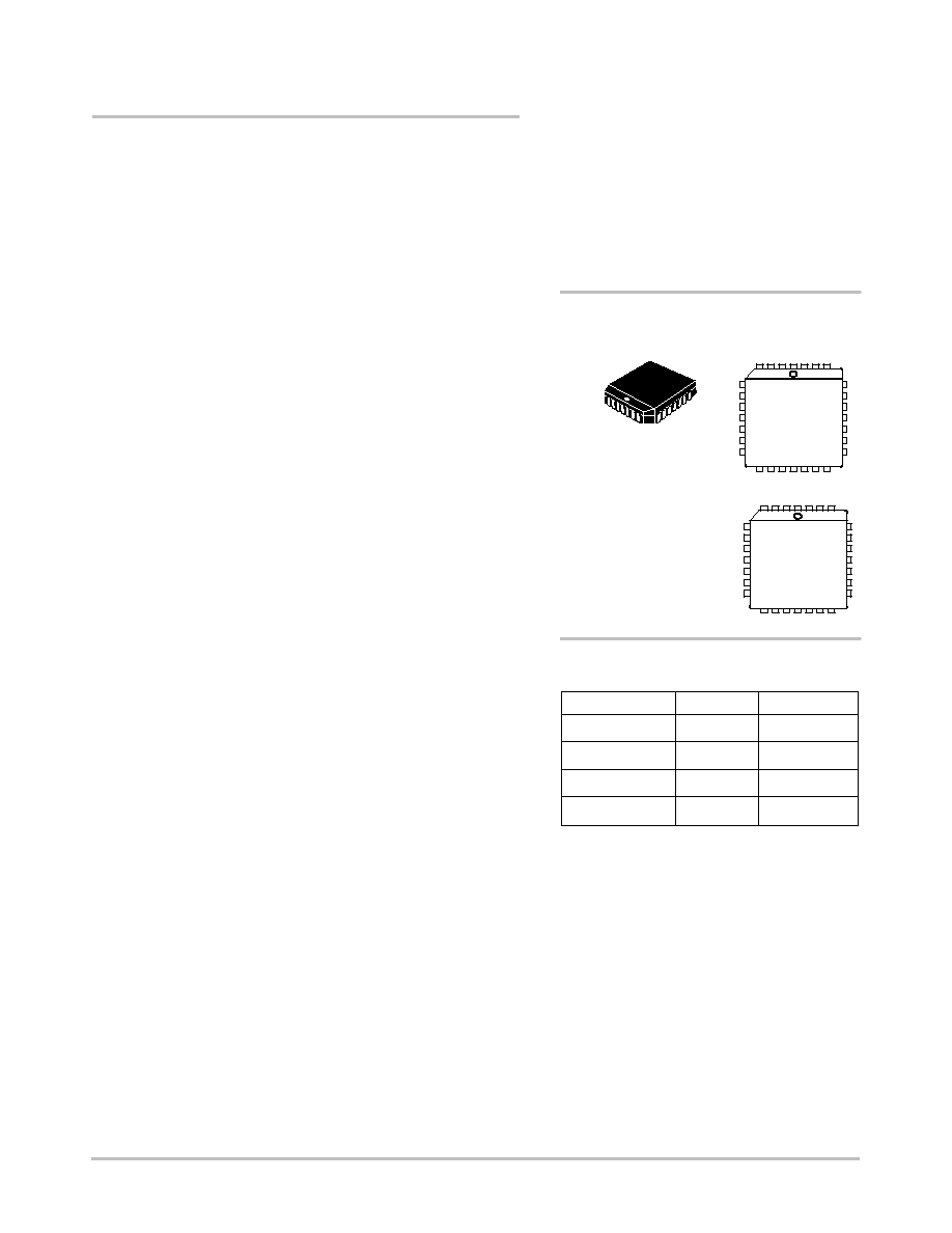
ORDERING INFORMATION
MC10E143FN
PLCC28
37 Units/Rail
MC10E143FNR2
PLCC28
500 Units/Reel
MC100E143FN
PLCC28
37 Units/Rail
MC100E143FNR2
PLCC28
500 Units/Reel
MARKING
DIAGRAMS
A
= Assembly Location
WL = Wafer Lot
YY = Year
WW = Work Week
PLCC28
FN SUFFIX
CASE 776
MC10E143FN
AWLYYWW
MC100E143FN
AWLYYWW
1 28
1 28
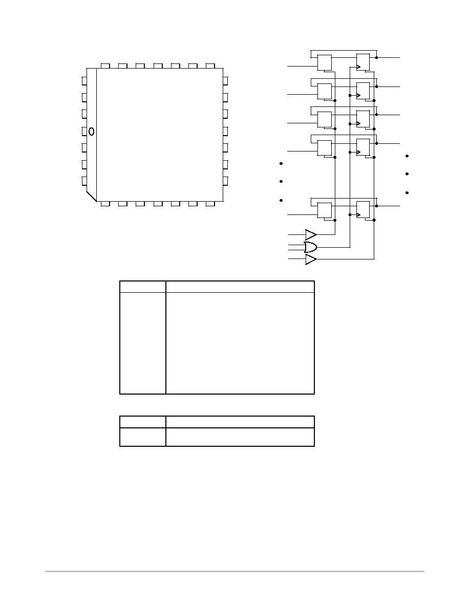
MUX
MUX
MUX
MUX
LOGIC DIAGRAM
D0
D1
D2
D3
D8
SEL
CLK1
CLK2
MR
Q0
Q1
Q2
Q3
Q8
MUX
D
R
D
D
D
D
R
R
R
R
MC10E143, MC100E143
http://onsemi.com
2
D2
D3
D4 VCCO Q0
Q1
Q2
VCCO
D5
D6
D7
D8
SEL
MR
CLK1
CLK2
VEE
NC
D0
D1
26
27
28
2
3
4
25
24
23
22
21
20
19
18
17
16
15
14
13
12
11
5
6
7
8
9
10
Q8
Q7
Q6
VCC
Q5
VCCO
Q4
Q3
1
Pinout: 28-Lead PLCC
(Top View)
* All VCC and VCCO pins are tied together on the die.
LOGIC DIAGRAM AND PINOUT ASSIGNMENT
Warning: All VCC, VCCO, and VEE pins must be externally
connected to Power Supply to guarantee proper operation.
PIN DESCRIPTION
PIN
FUNCTION
D0 D8
ECL Parallel Data Inputs
SEL
ECL Mode Select Input
CLK1, CLK2
ECL Clock Inputs
MR
ECL Master Reset
Q0 Q8
ECL Data Outputs
NC
No Connect
VCC, VCCO
Positive Supply
VEE
Negative Supply
FUNCTIONS
SEL
Mode
L
H
Load
Hold
MC10E143, MC100E143
http://onsemi.com
3
MAXIMUM RATINGS
(Note 1)
Symbol
Parameter
Condition 1
Condition 2
Rating
Units
VCC
PECL Mode Power Supply
VEE = 0 V
8
V
VEE
NECL Mode Power Supply
VCC = 0 V
8
V
VI
PECL Mode Input Voltage
VEE = 0 V
VI
VCC
6
V
I
C
ode
u
o age
NECL Mode Input Voltage
EE
0
VCC = 0 V
I
CC
VI
VEE
6
6
V
Iout
Output Current
Continuous
Surge
50
100
mA
mA
TA
Operating Temperature Range
0 to +85
°
C
Tstg
Storage Temperature Range
65 to +150
°
C
JA
Thermal Resistance (Junction to Ambient)
0 LFPM
500 LFPM
28 PLCC
28 PLCC
63.5
43.5
°
C/W
°
C/W
JC
Thermal Resistance (Junction to Case)
std bd
28 PLCC
22 to 26
°
C/W
VEE
PECL Operating Range
NECL Operating Range
4.2 to 5.7
5.7 to 4.2
V
V
Tsol
Wave Solder
<2 to 3 sec @ 248
°
C
265
°
C
1. Maximum Ratings are those values beyond which device damage may occur.
10E SERIES PECL DC CHARACTERISTICS
VCCx= 5.0 V; VEE= 0.0 V (Note 1)
0
°
C
25
°
C
85
°
C
Symbol
Characteristic
Min
Typ
Max
Min
Typ
Max
Min
Typ
Max
Unit
IEE
Power Supply Current
120
145
120
145
120
145
mA
VOH
Output HIGH Voltage (Note 2)
3980
4070
4160
4020
4105
4190
4090
4185
4280
mV
VOL
Output LOW Voltage (Note 2)
3050
3210
3370
3050
3210
3370
3050
3227
3405
mV
VIH
Input HIGH Voltage
3830
3995
4160
3870
4030
4190
3940
4110
4280
mV
VIL
Input LOW Voltage
3050
3285
3520
3050
3285
3520
3050
3302
3555
mV
IIH
Input HIGH Current
150
150
150
µ
A
IIL
Input LOW Current
0.5
0.3
0.5
0.25
0.3
0.2
µ
A
NOTE: Devices are designed to meet the DC specifications shown in the above table, after thermal equilibrium has been established. The
circuit is in a test socket or mounted on a printed circuit board and transverse air flow greater than 500 lfpm is maintained.
1. Input and output parameters vary 1:1 with VCC. VEE can vary +0.46 V / 0.06 V.
2. Outputs are terminated through a 50 ohm resistor to VCC2 volts.
10E SERIES NECL DC CHARACTERISTICS
VCCx= 0.0 V; VEE= 5.0 V (Note 1)
0
°
C
25
°
C
85
°
C
Symbol
Characteristic
Min
Typ
Max
Min
Typ
Max
Min
Typ
Max
Unit
IEE
Power Supply Current
120
145
120
145
120
145
mA
VOH
Output HIGH Voltage (Note 2)
1020
930
840
980
895
810
910
815
720
mV
VOL
Output LOW Voltage (Note 2)
1950
1790
1630
1950
1790
1630
1950
1773
1595
mV
VIH
Input HIGH Voltage
1170
1005
840
1130
970
810
1060
890
720
mV
VIL
Input LOW Voltage
1950
1715
1480
1950
1715
1480
1950
1698
1445
mV
IIH
Input HIGH Current
150
150
150
µ
A
IIL
Input LOW Current
0.5
0.3
0.5
0.065
0.3
0.2
µ
A
NOTE: Devices are designed to meet the DC specifications shown in the above table, after thermal equilibrium has been established. The
circuit is in a test socket or mounted on a printed circuit board and transverse air flow greater than 500 lfpm is maintained.
1. Input and output parameters vary 1:1 with VCC. VEE can vary +0.46 V / 0.06 V.
2. Outputs are terminated through a 50 ohm resistor to VCC2 volts.
MC10E143, MC100E143
http://onsemi.com
4
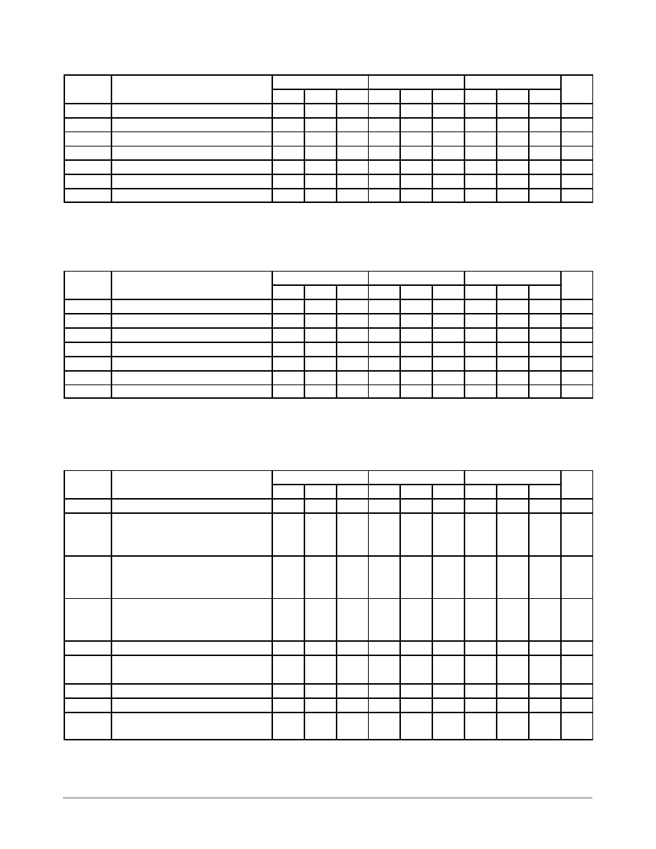
100E SERIES PECL DC CHARACTERISTICS
VCCx= 5.0 V; VEE= 0.0 V (Note 1)
0
°
C
25
°
C
85
°
C
Symbol
Characteristic
Min
Typ
Max
Min
Typ
Max
Min
Typ
Max
Unit
IEE
Power Supply Current
120
145
120
145
138
165
mA
VOH
Output HIGH Voltage (Note 2)
3975
4050
4120
3975
4050
4120
3975
4050
4120
mV
VOL
Output LOW Voltage (Note 2)
3190
3295
3380
3190
3255
3380
3190
3260
3380
mV
VIH
Input HIGH Voltage
3835
4050
4120
3835
4120
4120
3835
4120
4120
mV
VIL
Input LOW Voltage
3190
3300
3525
3190
3525
3525
3190
3525
3525
mV
IIH
Input HIGH Current
150
150
150
µ
A
IIL
Input LOW Current
0.5
0.3
0.5
0.25
0.5
0.2
µ
A
NOTE: Devices are designed to meet the DC specifications shown in the above table, after thermal equilibrium has been established. The
circuit is in a test socket or mounted on a printed circuit board and transverse air flow greater than 500 lfpm is maintained.
1. Input and output parameters vary 1:1 with VCC. VEE can vary +0.46 V / 0.8 V.
2. Outputs are terminated through a 50 ohm resistor to VCC2 volts.
100E SERIES NECL DC CHARACTERISTICS
VCCx= 0.0 V; VEE= 5.0 V (Note 1)
0
°
C
25
°
C
85
°
C
Symbol
Characteristic
Min
Typ
Max
Min
Typ
Max
Min
Typ
Max
Unit
IEE
Power Supply Current
120
145
120
145
138
165
mA
VOH
Output HIGH Voltage (Note 2)
1025
950
880
1025
950
880
1025
950
880
mV
VOL
Output LOW Voltage (Note 2)
1810
1705
1620
1810
1745
1620
1810
1740
1620
mV
VIH
Input HIGH Voltage
1165
950
880
1165
880
880
1165
880
880
mV
VIL
Input LOW Voltage
1810
1700
1475
1810
1475
1475
1810
1475
1475
mV
IIH
Input HIGH Current
150
150
150
µ
A
IIL
Input LOW Current
0.5
0.3
0.5
0.25
0.5
0.2
µ
A
NOTE: Devices are designed to meet the DC specifications shown in the above table, after thermal equilibrium has been established. The
circuit is in a test socket or mounted on a printed circuit board and transverse air flow greater than 500 lfpm is maintained.
1. Input and output parameters vary 1:1 with VCC. VEE can vary +0.46 V / 0.8 V.
2. Outputs are terminated through a 50 ohm resistor to VCC2 volts.
AC CHARACTERISTICS
VCCx= 5.0 V; VEE= 0.0 V or VCCx= 0.0 V; VEE= 5.0 V (Note 1)
0
°
C
25
°
C
85
°
C
Symbol
Characteristic
Min
Typ
Max
Min
Typ
Max
Min
Typ
Max
Unit
fMAX
Maximum Toggle Frequency
TBD
TBD
TBD
GHz
tPLH
Propagation Delay to Output
ps
tPHL
Clk
600
800
1000
600
800
1000
600
800
1000
MR
600
800
1000
600
800
1000
600
800
1000
ts
Setup Time
ps
D
50
100
50
100
50
100
SEL
300
150
300
150
300
150
th
Hold Time
ps
D
300
100
300
100
300
100
SEL
75
150
75
150
75
150
tRR
Reset Recovery Time
900
700
900
700
900
700
ps
tPW
Minimum Pulse Width
ps
Clk, MR
400
400
400
tSKEW
Within-Device Skew (Note 1.)
75
75
75
ps
tJITTER
CycletoCycle Jitter
TBD
TBD
TBD
ps
tr
Rise/Fall Times
ps
tf
(20 - 80%)
300
525
800
300
525
800
300
525
800
1. 10 Series: VEE can vary +0.46 V / 0.06 V.
100 Series: VEE can vary +0.46 V / 0.8 V.
1. Within-device skew is defined as identical transitions on similar paths through a device.
MC10E143, MC100E143
http://onsemi.com
5
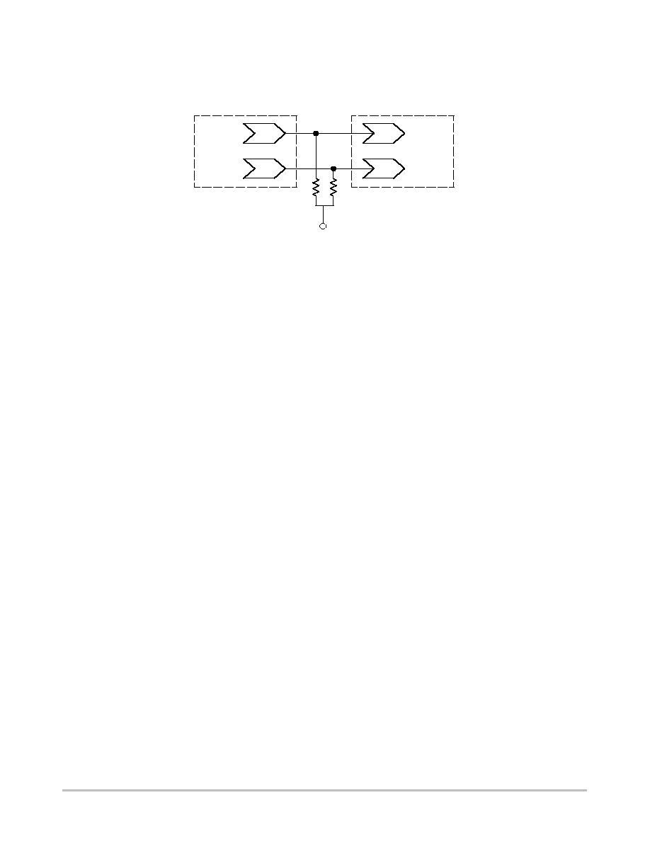
Figure 1. Typical Termination for Output Driver and Device Evaluation
(See Application Note AND8020 Termination of ECL Logic Devices.)
W
Driver
Device
Receiver
Device
Q
Qb
D
Db
50
W
50
V TT
VTT = VCC 2.0 V
Resource Reference of Application Notes
AN1404
ECLinPS Circuit Performance at NonStandard VIH Levels
AN1405
ECL Clock Distribution Techniques
AN1406
Designing with PECL (ECL at +5.0 V)
AN1503
ECLinPS I/O SPICE Modeling Kit
AN1504
Metastability and the ECLinPS Family
AN1568
Interfacing Between LVDS and ECL
AN1596
ECLinPS Lite Translator ELT Family SPICE I/O Model Kit
AN1650
Using WireOR Ties in ECLinPS Designs
AN1672
The ECL Translator Guide
AND8001
Odd Number Counters Design
AND8002
Marking and Date Codes
AND8020
Termination of ECL Logic Devices