Äîêóìåíòàöèÿ è îïèñàíèÿ www.docs.chipfind.ru
Semiconductor Components Industries, LLC, 2005
January, 2005 - Rev. 6
1
Publication Order Number:
MBRD835L/D
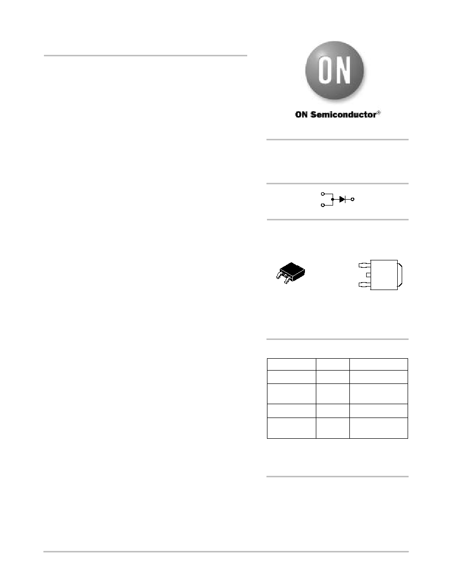
MBRD835L
Preferred Device
SWITCHMODE]
Power Rectifier
DPAK Surface Mount Package
This SWITCHMODE power rectifier which uses the Schottky
Barrier principle with a proprietary barrier metal, is designed for use
as output rectifiers, free wheeling, protection and steering diodes in
switching power supplies, inverters and other inductive switching
circuits.
Features
·
Low Forward Voltage
·
125
°C Operating Junction Temperature
·
Epoxy Meets UL 94 V-0 @ 0.125 in
·
Compact Size
·
Lead Formed for Surface Mount
·
Pb-Free Packages are Available
Mechanical Characteristics
·
Case: Epoxy, Molded
·
Weight: 0.4 Gram (Approximately)
·
Finish: All External Surfaces Corrosion Resistant and Terminal
Leads are Readily Solderable
·
Lead and Mounting Surface Temperature for Soldering Purposes:
260
°C Max. for 10 Seconds
·
Shipped 75 Units Per Plastic Tube
·
Available in 16 mm Tape and Reel, 2500 Units Per 13 in Reel, by
Adding a "T4" Suffix to the Part Number
Device
Package
Shipping
ORDERING INFORMATION
SCHOTTKY BARRIER
RECTIFIER
8.0 AMPERES, 35 VOLTS
Preferred devices are recommended choices for future use
and best overall value.
MBRD835L
DPAK
75 Units/Rail
MBRD835LT4
DPAK
2500/Tape & Reel
4
1
3
For information on tape and reel specifications,
including part orientation and tape sizes, please
refer to our Tape and Reel Packaging Specifications
Brochure, BRD8011/D.
MBRD835LT4G
DPAK
(Pb-Free)
2500/Tape & Reel
DPAK
CASE 369C
MARKING
DIAGRAM
Y
= Year
WW
= Work Week
1 2
3
4
YWW
B
835L
MBRD835LG
DPAK
(Pb-Free)
75 Units/Rail
http://onsemi.com
MBRD835L
http://onsemi.com
2
MAXIMUM RATINGS
Rating
Symbol
Value
Unit
Peak Repetitive Reverse Voltage
Working Peak Reverse Voltage
DC Blocking Voltage
V
RRM
V
RWM
V
R
35
V
Average Rectified Forward Current
(At Rated V
R
, T
C
= 88°C)
I
F(AV)
8.0
A
Peak Repetitive Forward Current
(At Rated V
R
, Square Wave, 20 kHz, T
C
= 80°C)
I
FRM
16
A
Non-Repetitive Peak Surge Current
(Surge applied at rated load conditions, halfwave, single phase, 60 Hz)
I
FSM
75
A
Repetitive Avalanche Current
(Current Decaying Linearly to Zero in 1 ms, Frequency Limited by T
Jmax
)
I
AR
2.0
A
Storage / Operating Case Temperature
T
stg
-65 to +150
°C
Operating Junction Temperature
T
J
-65 to +125
°C
Voltage Rate of Change (Rated V
R
)
dv/dt
10,000
V/ms
Maximum ratings are those values beyond which device damage can occur. Maximum ratings applied to the device are individual stress limit
values (not normal operating conditions) and are not valid simultaneously. If these limits are exceeded, device functional operation is not
implied, damage may occur and reliability may be affected.
THERMAL CHARACTERISTICS
Rating
Symbol
Value
Unit
Thermal Resistance - Junction-to-Case
R
qJC
2.8
°C/W
Thermal Resistance - Junction-to-Ambient (Note 1)
R
qJA
80
°C/W
ELECTRICAL CHARACTERISTICS
Maximum Instantaneous Forward Voltage (Note 2) (i
F
= 8 Amps, T
C
= +25°C)
(i
F
= 8 Amps, T
C
= +125°C)
V
F
0.51
0.41
V
Maximum Instantaneous Reverse Current (Note 2) (Rated dc Voltage, T
C
= +25°C)
(Rated dc Voltage, T
C
= +100°C)
I
R
1.4
35
mA
1. Rating applies when surface mounted on the minimum pad size recommended.
2. Pulse Test: Pulse Width = 300 ms, Duty Cycle 2%.
MBRD835L
http://onsemi.com
3
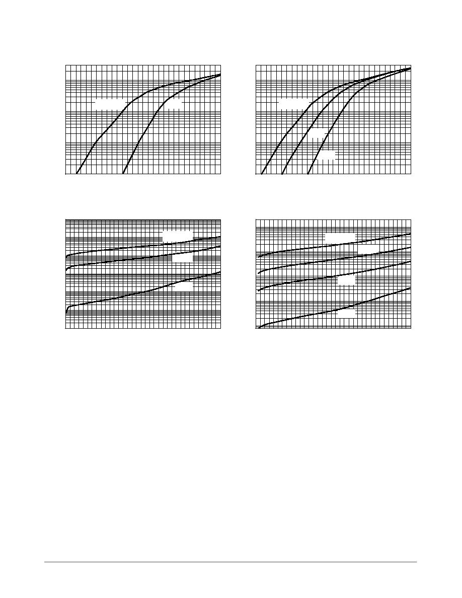
TYPICAL CHARACTERISTICS
10
1
0.1
0
0.6
v
F
, INSTANTANEOUS VOLTAGE (VOLTS)
Figure 1. Maximum Forward Voltage
Figure 2. Typical Forward Voltage
i F
, INST
ANT
ANEOUS FOR
W
ARD CURRENT
(mA
)
0.01
0.1
0.2
0.3
0.4
0.5
T
J
= 125°C
25°C
10
1
0.1
0
0.6
V
F
, INSTANTANEOUS VOLTAGE (VOLTS)
0.01
0.1
0.2
0.3
0.4
0.5
75°C
I F
, INST
ANT
ANEOUS FOR
W
ARD CURRENT
(AMP
S
25°C
T
J
= 125°C
10
1
0.1
0
35
V
F
, REVERSE VOLTAGE (VOLTS)
Figure 3. Maximum Reverse Current
Figure 4. Typical Reverse Current
0.001
5
10
15
20
T
J
= 125°C
25°C
10
1
0.1
0
V
R
, REVERSE VOLTAGE (VOLTS)
0.01
5
10
15
20
T
J
= 125°C
75°C
25°C
I R
, REVERSE CURRENT
(mA)
I R
, REVERSE CURRENT
(mA)
0.01
100
1000
100
100°C
100°C
25
30
25
30
35
MBRD835L
http://onsemi.com
4
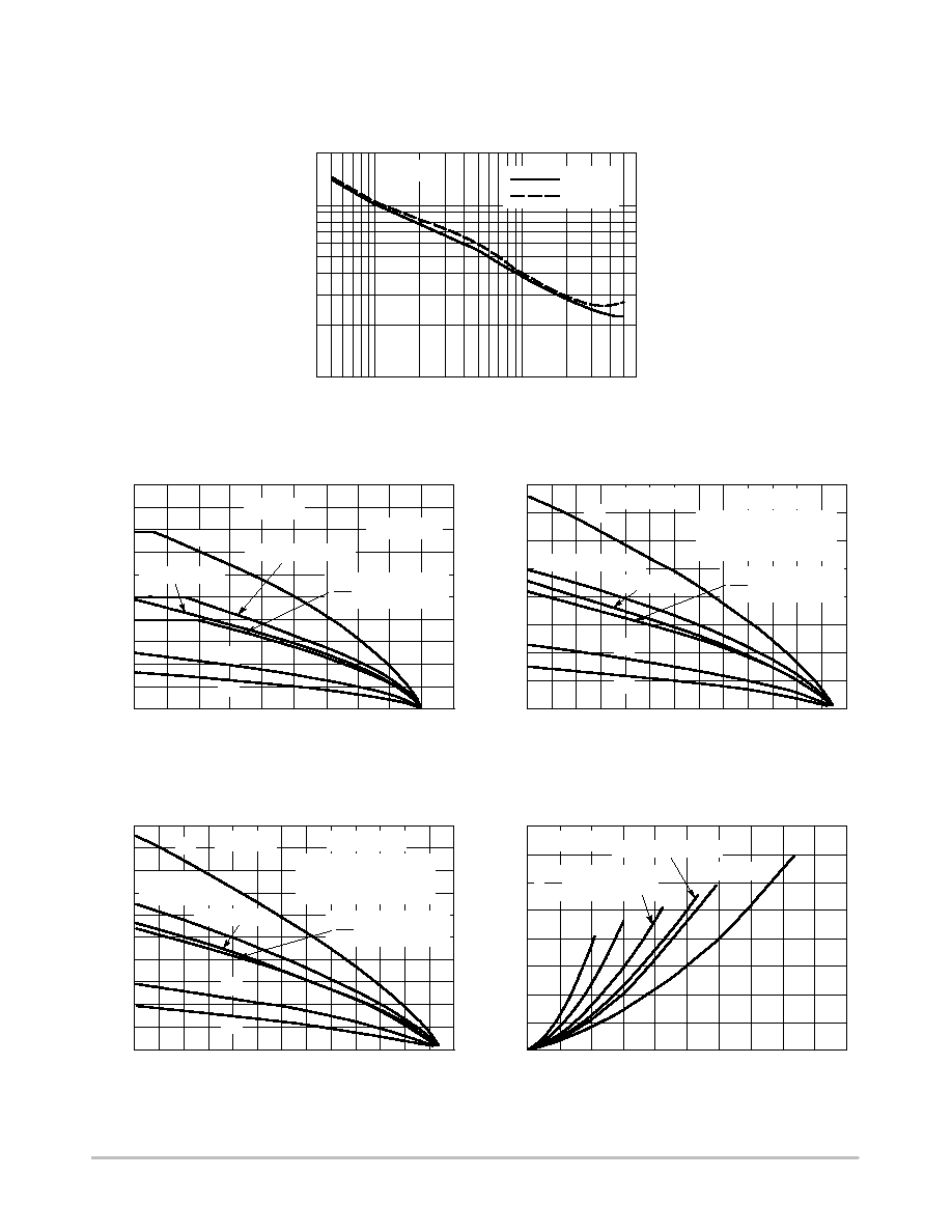
TYPICAL CHARACTERISTICS
16
80
130
T
C
, CASE TEMPERATURE (°C)
0
8
7
6
0
130
T
A
, AMBIENT TEMPERATURE (°C)
0
T
J
= 125°C
I F(A
V)
,
A
VERAGE FOR
W
ARD CURRENT
(AMPS) 14.4
12.8
11.2
9.6
8
6.4
4.8
3.2
1.6
85
90
95
100
105
110
115
120
125
dc
SQUARE WAVE
IPK
IAV
+ 5
(CAPACITIVE
LOAD)
10
20
I F(A
V)
,
A
VERAGE FOR
W
ARD CURRENT
(AMPS)
5
4
3
2
1
50
10
20 30
40
80
60 70
100
90
110 120
dc
p (RESISTIVE LOAD)
SQUARE WAVE
10
20
p (RESISTIVE LOAD)
T
J
= 125°C
IPK
IAV
+ 5
(CAPACITIVE
LOAD)
R
qJA
= 40°C/W
SURFACE MOUNTED ON
MINIMUM RECOMMENDED
PAD SIZE
R
qJA
= 6°C/W
Figure 5. Maximum and Typical Capacitance
1
V
R
, REVERSE VOLTAGE (VOLTS)
100
10
1000
C, CAP
ACIT
ANCE (pF)
TYPICAL
MAXIMUM
T
J
= 25°C
Figure 6. Current Derating, Infinite Heatsink
Figure 7. Current Derating
4
3.5
0
T
A
, AMBIENT TEMPERATURE (°C)
0
0
I
F(AV)
, AVERAGE FORWARD CURRENT (AMPS)
1.5
3
4.5
6
4.5
5
I F(A
V)
,
A
VERAGE FOR
W
ARD CURRENT
(AMPS)
3
2.5
2
1.5
1
0.5
130
50
20 30
40
80
60 70
100
90
110 120
T
J
= 125°C
dc
p
(RESISTIVE LOAD)
SQUARE WAVE
10
20
P
F(A
V)
,
A
VERAGE FOR
W
ARD POWER DISSIP
A
TION (W
A
T
T
8
7
6
0
5
4
3
2
1
7.5
9
10.5
12
13.5
15
T
J
= 125°C
dc
p (RESISTIVE LOAD)
SQUARE WAVE
10
20
IPK
IAV
+ 5
(CAPACITIVE
LOAD)
R
qJA
= 80°C/W
SURFACE MOUNTED ON
MINIMUM RECOMMENDED
PAD SIZE
IPK
IAV
+ 5
(CAPACITIVE
LOAD)
10
Figure 8. Current Derating, Free Air
Figure 9. Forward Power Dissipation
MBRD835L
http://onsemi.com
5
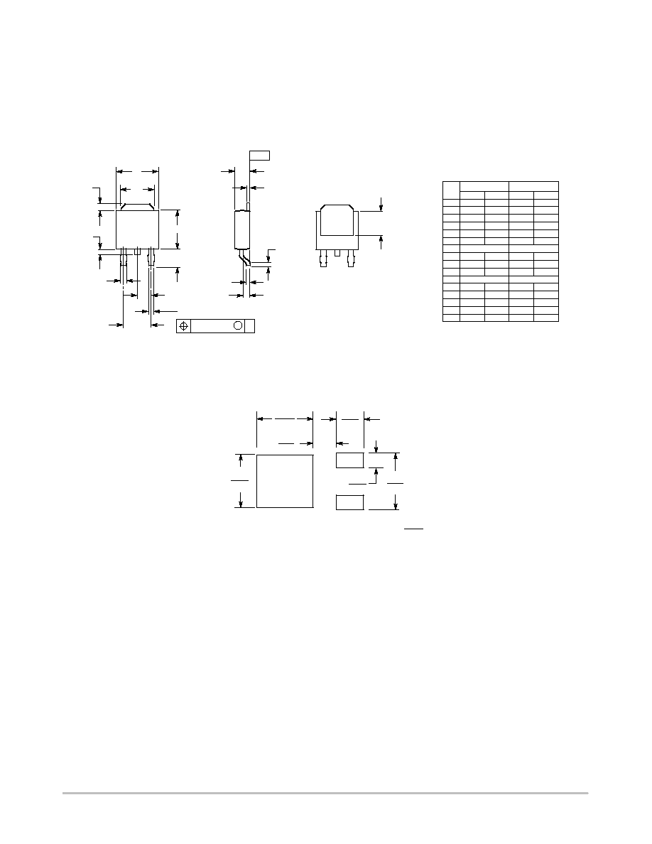
PACKAGE DIMENSIONS
DPAK
CASE 369C
ISSUE O
D
A
K
B
R
V
S
F
L
G
2 PL
M
0.13 (0.005)
T
E
C
U
J
H
-T-
SEATING
PLANE
Z
DIM
MIN
MAX
MIN
MAX
MILLIMETERS
INCHES
A
0.235
0.245
5.97
6.22
B
0.250
0.265
6.35
6.73
C
0.086
0.094
2.19
2.38
D
0.027
0.035
0.69
0.88
E
0.018
0.023
0.46
0.58
F
0.037
0.045
0.94
1.14
G
0.180 BSC
4.58 BSC
H
0.034
0.040
0.87
1.01
J
0.018
0.023
0.46
0.58
K
0.102
0.114
2.60
2.89
L
0.090 BSC
2.29 BSC
R
0.180
0.215
4.57
5.45
S
0.025
0.040
0.63
1.01
U
0.020
---
0.51
---
V
0.035
0.050
0.89
1.27
Z
0.155
---
3.93
---
NOTES:
1. DIMENSIONING AND TOLERANCING
PER ANSI Y14.5M, 1982.
2. CONTROLLING DIMENSION: INCH.
1
2
3
4
5.80
0.228
2.58
0.101
1.6
0.063
6.20
0.244
3.0
0.118
6.172
0.243
mm
inches
SCALE 3:1
*For additional information on our Pb-Free strategy and soldering
details, please download the ON Semiconductor Soldering and
Mounting Techniques Reference Manual, SOLDERRM/D.
SOLDERING FOOTPRINT*