®
Semiconductor Components Industries, LLC, 2003
May, 2003 - Rev. 3
1
Publication Order Number:
MBRB4030/D
MBRB4030
Preferred Device
SWITCHMODE
TM
Power Rectifier
Using the Schottky Barrier principle with a proprietary barrier
metal. These state-of-the-art devices have the following features:
À
Guardring for Stress Protection
À
Maximum Die Size
À
150
░
C Operating Junction Temperature
À
Short Heat Sink Tab Manufactured - Not Sheared
Mechanical Characteristics
À
Case: Epoxy, Molded, Epoxy Meets UL94, VO
À
Weight: 1.7 Grams (approximately)
À
Finish: All External Surfaces Corrosion Resistant and Terminal
Leads Readily Solderable
À
Shipped 50 Units per Plastic Tube
À
Available in 24 mm Tape and Reel, 800 Units per 13
Reel by Adding
a "T4" Suffix to the Part Number
À
Marking: B4030
À
Device Meets MSL1 Requirements
À
ESD Ratings:
Machine Model, C (>400 V)
Human Body Model, 3B (>8000 V)
MAXIMUM RATINGS
Rating
Symbol
Value
Unit
Peak Repetitive Reverse Voltage
Working Peak Reverse Voltage
DC Blocking Voltage
V
RRM
V
RWM
V
R
30
V
Average Rectified Forward Current
(At Rated V
R
) T
C
= +115
░
C (Note 1.)
I
F(AV)
40
A
Peak Repetitive Forward Current
(At Rated V
R
, Square Wave,
20 kHz) T
C
= +112
░
C
I
FRM
80
A
Non-Repetitive Peak Surge Current
(Surge Applied at Rated Load
Conditions Halfwave, Single
Phase, 60 Hz)
I
FSM
300
A
Peak Repetitive Reverse Surge
Current (2.0
m
s, 1.0 kHz)
I
RRM
2.0
A
Storage Temperature Range
T
stg
-65 to
+150
░
C
Operating Junction
Temperature Range
T
J
-65 to
+150
░
C
Voltage Rate of Change
(Rated V
R
)
dv/dt
10,000
V/
m
s
Reverse Energy
(Unclamped Inductive Surge)
(T
C
= 25
░
C, L = 3.0 mH)
W
600
mJ
1. Rating applies when pins 1 and 3 are connected.
Device
Package
Shipping
ORDERING INFORMATION
MBRB4030
D
2
PAK
D
2
PAK
CASE 418B
STYLE 3
50/Rail
3
4
1
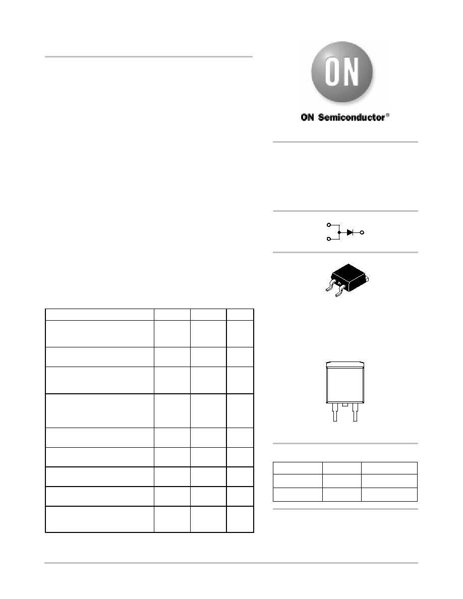
SCHOTTKY BARRIER
RECTIFIER
40 AMPERES
30 VOLTS
Preferred devices are recommended choices for future use
and best overall value.
3
1
4
MBRB4030T4
D
2
PAK
800/Tape & Reel
MARKING DIAGRAM
B4030
B4030 = Device Code
http://onsemi.com
MBRB4030
http://onsemi.com
2
THERMAL CHARACTERISTICS
Characteristic
Symbol
Value
Unit
Thermal Resistance - Junction to Case
R
JC
1.0
░
C/W
Thermal Resistance - Junction to Ambient
(Note 3.)
R
JA
50
░
C/W
ELECTRICAL CHARACTERISTICS
Maximum Instantaneous Forward Voltage (Notes 2. and 4.), per Device
(I
F
= 20 A, T
C
= + 25
░
C)
(I
F
= 20 A, T
C
= +150
░
C)
(I
F
= 40 A, T
C
= + 25
░
C)
(I
F
= 40 A, T
C
= +150
░
C)
V
F
0.46
0.34
0.55
0.45
V
Maximum Instantaneous Reverse Current (Note 4.), per Device
(Rated DC Voltage, T
C
= + 25
░
C)
(Rated DC Voltage, T
C
= +125
░
C)
I
R
0.35
150
mA
2. Rating applies when pins 1 and 3 are connected.
3. Rating applies when surface mounted on the miniumum pad size recommended.
4. Pulse Test: Pulse Width = 300
Á
s, Duty Cycle
2.0%
MBRB4030
http://onsemi.com
3
ELECTRICAL CHARACTERISTICS
V
R
, REVERSE VOLTAGE (V)
V
R
, REVERSE VOLTAGE (V)
I R
, REVERSE CURRENT
(A)
I F
, INST
ANT
ANEOUS FOR
W
ARD CURRENT
(mA)
(PIN 1 SHOR
TED
T
O
PIN 3)
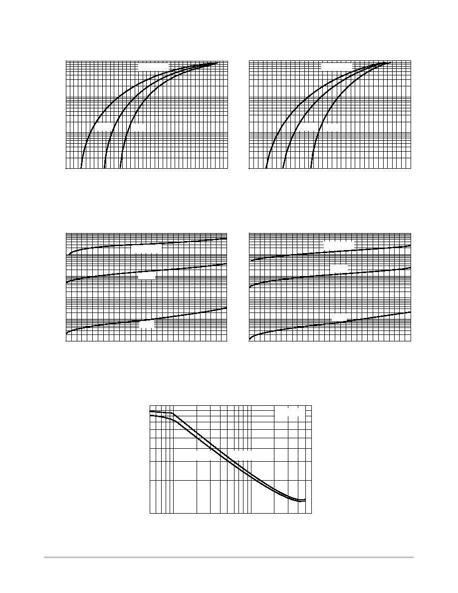
Figure 1. Maximum Forward Voltage
V
F
, INSTANTANEOUS VOLTAGE (V)
100
10
1.0
0.1
0.8
0.6
0.4
0.2
0
Figure 2. Typical Forward Voltage
V
F
, INSTANTANEOUS VOLTAGE (V)
100
10
1.0
0.1
0.7
0.6
0.4
0.1
0
Figure 3. Maximum Reverse Current
V
R
, REVERSE VOLTAGE (V)
1.0
0.1
0.01
10
-3
10
-4
10
-5
30
25
15
10
0
Figure 4. Typical Reverse Current
1.0
0.1
0.01
10
-3
10
-4
10
-5
30
25
10
0
I R
, REVERSE CURRENT
(A)
0.7
0.5
0.3
0.1
0.5
0.3
0.2
20
5
20
15
5
Figure 5. Maximum and Typical Capacitance
10
4
1000
10
C, CAP
ACIT
ANCE (pF)
1
TYPICAL
25
░
C
T
J
= 150
░
C
100
░
C
T
J
= 25
░
C
25
░
C
T
J
= 150
░
C
100
░
C
25
░
C
T
J
= 150
░
C
100
░
C
25
░
C
T
J
= 150
░
C
100
░
C
I F
, INST
ANT
ANEOUS FOR
W
ARD CURRENT
(mA)
(PIN 1 SHOR
TED
T
O
PIN 3)
MAXIMUM
MBRB4030
http://onsemi.com
4
ELECTRICAL CHARACTERISTICS
I
F(AV)
, AVERAGE FORWARD CURRENT (A)
50
40
30
20
10
0
70
50
30
P F(A
V)
,
A
VERAGE FOR
W
ARD POWER DISSIP
A
TION (W
A
TTS)
60
40
80
DC
10
(PIN 1 SHOR
TED
T
O
PIN 3)
T
A
, AMBIENT TEMPERATURE (
░
C)
I F(A
V)
,
A
VERAGE FOR
W
ARD CURRENT
(A)
(PIN 1 SHOR
TED
T
O
PIN 3)
T
A
, AMBIENT TEMPERATURE (
░
C)
20
15
10
5
0
50
I F(A
V)
,
A
VERAGE FOR
W
ARD CURRENT
(A)
100
DC
10
20
SQUARE WAVE
(PIN 1 SHOR
TED
T
O
PIN 3)
150
12
10
8
6
2
0
150
100
0
50
t, TIME (ms)
1.0
0.1
0.01
100
0.1
R(t), EFFECTIVE
TRANSIENT
THERMAL
10
1.0
1000
SINGLE PULSE
RESIST
ANCE (NORMALIZED)
SURFACE MOUNTED ON
MINIMUM RECOMMENDED
PAD SIZE
R
JA
= 25
░
C/W
4
SQUARE WAVE
20
0
10
I
PK
I
AV
= 5.0 (CAPACITIVE
LOAD)
I
PK
I
AV
= 5.0 (CAPACITIVE
LOAD)
(RESISTIVE LOAD)
I
PK
I
AV
= 5.0 (CAPACITIVE
LOAD)
20
T
J
= 150
░
C
10
20
DC
(RESISTIVE LOAD)
R
JA
= 50
░
C/W
(RESISTIVE LOAD)
SQUARE WAVE
T
C
, CASE TEMPERATURE (
░
C)
70
50
40
30
20
10
0
140
120
100
I F(A
V)
,
A
VERAGE FOR
W
ARD CURRENT
(A)
130
110
150
10
20
SQUARE WAVE
(PIN 1 SHOR
TED
T
O
PIN 3)
60
DC
I
PK
I
AV
= 5.0
(RESISTIVE LOAD)
(CAPACITIVE
LOAD)
P
pk
P
pk
t
p
t
1
TIME
DUTY CYCLE, D = t
p
/t
1
PEAK POWER, P
pk
, is peak of an
equivalent square power pulse.
T
JL
= P
pk
À
R
JL
[D + (1 - D)
À
r(t
1
+ t
p
) + r(t
p
) - r(t
1
)]
where
T
JL
= the increase in junction temperature above the lead temperature
r(t) = normalized value of transient thermal resistance at time, t, for example,
r(t) =
r(t
1
+ t
p
) = normalized value of transient thermal resistance at time, t
1
+ t
p
.
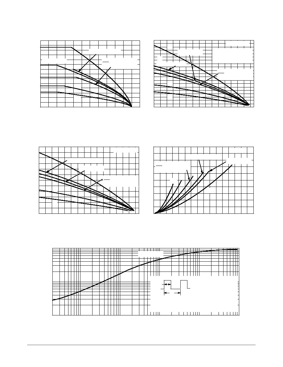
Figure 6. Current Derating, Infinite Heatsink
Figure 7. Current Derating
Figure 8. Current Derating, Free Air
Figure 9. Forward Power Dissipation
Figure 10. Thermal Response
MBRB4030
http://onsemi.com
5
INFORMATION FOR USING THE D
2
PAK SURFACE MOUNT PACKAGE
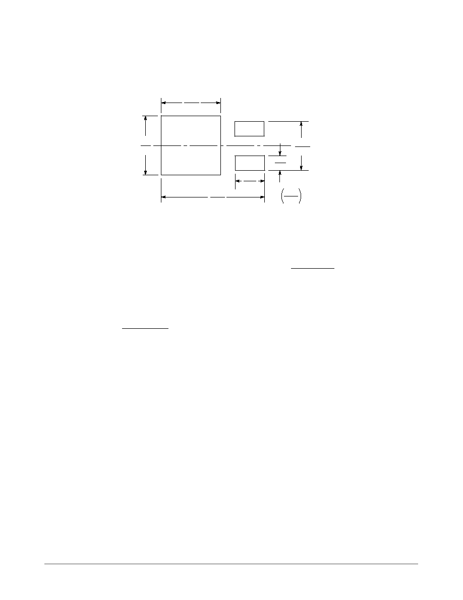
MINIMUM RECOMMENDED FOOTPRINTS FOR SURFACE MOUNTED APPLICATIONS
Surface mount board layout is a critical portion of the
total design. The footprint for the semiconductor packages
must be the correct size to insure proper solder connection
interface between the board and the package. With the
correct pad geometry, the packages will self align when
subjected to a solder reflow process.
mm
inches
0.33
8.38
0.04
1.016
0.67
17.02
0.42
10.66
0.12
3.05
0.24
6.096
D
2
PAK POWER DISSIPATION
The power dissipation of the D
2
PAK is a function of the
drain pad size. This can vary from the minimum pad size
for soldering to a pad size given for maximum power
dissipation. Power dissipation for a surface mount device is
determined by T
J(max)
, the maximum rated junction
temperature of the die, R
JA
, the thermal resistance from
the device junction to ambient; and the operating
temperature, T
A
. Using the values provided on the data
sheet for the D
2
PAK package, P
D
can be calculated as
follows:
P
D
=
T
J(max)
- T
A
R
JA
The values for the equation are found in the maximum
ratings table on the data sheet. Substituting these values
into the equation for an ambient temperature T
A
of 25
░
C,
one can calculate the power dissipation of the device which
in this case is 2.5 watts.
P
D
= 150
░
C - 25
░
C = 2.5 watts
50
░
C/W
The 50
░
C/W for the D
2
PAK package assumes the
recommended drain pad area of 158K mil
2
on FR-4 glass
epoxy printed circuit board to achieve a power dissipation
of 2.5 watts using the footprint shown. Another alternative
is to use a ceramic substrate or an aluminum core board
such as Thermal Clad
TM
. By using an aluminum core board
material such as Thermal Clad, the power dissipation can
be doubled using the same footprint.
GENERAL SOLDERING PRECAUTIONS
The melting temperature of solder is higher than the rated
temperature of the device. When the entire device is heated
to a high temperature, failure to complete soldering within
a short time could result in device failure. Therefore, the
following items should always be observed in order to
minimize the thermal stress to which the devices are
subjected.
À
Always preheat the device.
À
The delta temperature between the preheat and
soldering should be 100
░
C or less.*
À
When preheating and soldering, the temperature of the
leads and the case must not exceed the maximum
temperature ratings as shown on the data sheet. When
using infrared heating with the reflow soldering
method, the difference shall be a maximum of 10
░
C.
À
The soldering temperature and time shall not exceed
260
░
C for more than 5 seconds.
À
When shifting from preheating to soldering, the
maximum temperature gradient shall be 5
░
C or less.
À
After soldering has been completed, the device should
be allowed to cool naturally for at least three minutes.
Gradual cooling should be used as the use of forced
cooling will increase the temperature gradient and
result in latent failure due to mechanical stress.
À
Mechanical stress or shock should not be applied
during cooling
* * Soldering a device without preheating can cause
excessive thermal shock and stress which can result in
damage to the device.
* * Due to shadowing and the inability to set the wave
height to incorporate other surface mount components, the
D
2
PAK is not recommended for wave soldering.