MAC15A4 (1) VIEW
ę
Semiconductor Components Industries, LLC, 1999
February, 2000 ş Rev. 1
1
Publication Order Number:
MAC15A4/D
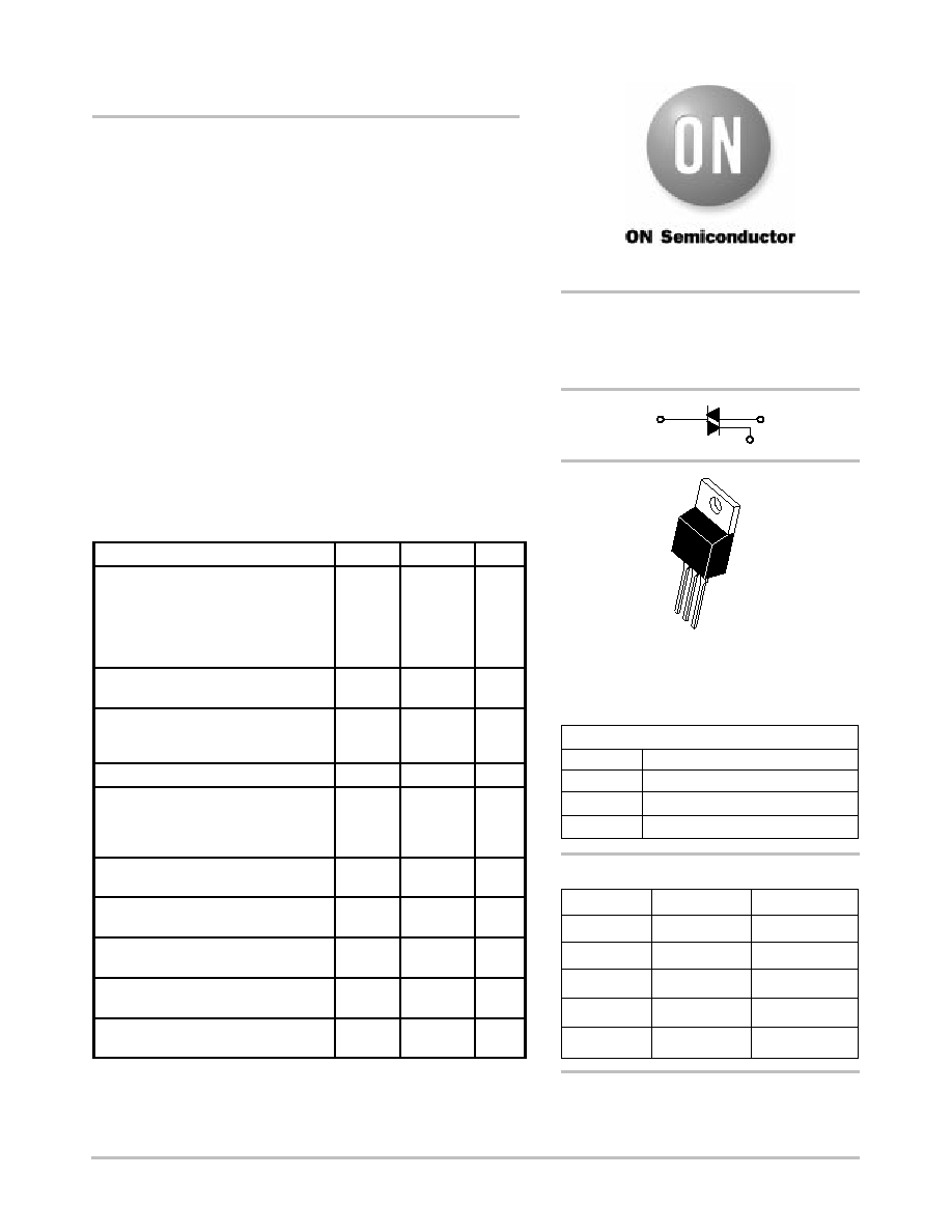
MAC15 Series
Preferred Device
Triacs
Silicon Bidirectional Thyristors
Designed primarily for full-wave ac control applications, such as
solidşstate relays, motor controls, heating controls and power
supplies; or wherever fullşwave silicon gate controlled solidşstate
devices are needed. Triac type thyristors switch from a blocking to a
conducting state for either polarity of applied main terminal voltage
with positive or negative gate triggering.
Ě
Blocking Voltage to 800 Volts
Ě
All Diffused and Glass Passivated Junctions for Greater Parameter
Uniformity and Stability
Ě
Small, Rugged, Thermowatt Construction for Low Thermal
Resistance, High Heat Dissipation and Durability
Ě
Gate Triggering Guaranteed in Three Modes (MAC15 Series) or
Four Modes (MAC15A Series)
Ě
Device Marking: Logo, Device Type, e.g., MAC15A6, Date Code
MAXIMUM RATINGS
(TJ = 25
░
C unless otherwise noted)
Rating
Symbol
Value
Unit
Peak Repetitive OffşState Voltage(1)
(TJ = ş40 to +125
░
C, Sine Wave 50 to
60 Hz, Gate Open)
MAC15A6
MAC15ş8, MAC15A8
MAC15ş10, MAC15A10
VDRM,
VRRM
400
600
800
Volts
Peak Gate Voltage
(Pulse Width
v
1.0
Á
sec; TC = 90
░
C)
VGM
10
Volts
OnşState Current RMS
Full Cycle Sine Wave 50 to 60 Hz
(TC = +90
░
C)
IT(RMS)
15
A
Circuit Fusing Consideration (t = 8.3 ms)
I2t
93
A2s
Peak Nonşrepetitive Surge Current
(One Full Cycle Sine Wave,
60 Hz, TC = +80
░
C)
Preceded and followed by rated current
ITSM
150
A
Peak Gate Power (TC = +80
░
C,
Pulse Width = 1.0
Á
s)
PGM
20
Watts
Average Gate Power
(TC = +80
░
C, t = 8.3 ms)
PG(AV)
0.5
Watts
Peak Gate Current
(Pulse Width
v
1.0
Á
sec; TC = 90
░
C)
IGM
2.0
A
Operating Junction Temperature Range
TJ
ş 40 to
+125
░
C
Storage Temperature Range
Tstg
ş 40 to
+150
░
C
(1) VDRM and VRRM for all types can be applied on a continuous basis. Blocking
voltages shall not be tested with a constant current source such that the
voltage ratings of the devices are exceeded.
TRIACS
15 AMPERES RMS
400 thru 800 VOLTS
Device
Package
Shipping
ORDERING INFORMATION
MAC15ş8
TO220AB
500/Box
MAC15ş10
TO220AB
MAC15A6
TO220AB
TOş220AB
CASE 221A
STYLE 4
1
2
3
4
PIN ASSIGNMENT
1
2
3
Gate
Main Terminal 1
Main Terminal 2
4
Main Terminal 2
http://onsemi.com
500/Box
500/Box
MT1
G
MT2
MAC15A8
TO220AB
500/Box
MAC15A10
TO220AB
500/Box
Preferred devices are recommended choices for future use
and best overall value.
MAC15 Series
http://onsemi.com
2
THERMAL CHARACTERISTICS
Characteristic
Symbol
Value
Unit
Thermal Resistance -- Junction to Case
Thermal Resistance
-- Junction to Ambient
R
JC
R
JA
2.0
62.5
░
C/W
Maximum Lead Temperature for Soldering Purposes 1/8
from Case for 10 Seconds
TL
260
░
C
ELECTRICAL CHARACTERISTICS
(TC = 25
░
C unless otherwise noted; Electricals apply in both directions)
Characteristic
Symbol
Min
Typ
Max
Unit
OFF CHARACTERISTICS
Peak Blocking Current
TJ = 25
░
C
(VD = Rated VDRM, VRRM; Gate Open)
TJ = 125
░
C
IDRM,
IRRM
--
--
--
--
10
2.0
Á
A
mA
ON CHARACTERISTICS
Peak OnşState Voltage(1) (ITM =
"
21 A Peak)
VTM
--
1.3
1.6
Volts
Gate Trigger Current (Continuous dc)
(VD = 12 Vdc, RL = 100 Ohms)
MT2(+), G(+)
MT2(+), G(ş)
MT2(ş), G(ş)
MT2(ş), G(+) "A'' SUFFIX ONLY
IGT
--
--
--
--
--
--
--
--
50
50
50
75
mA
Gate Trigger Voltage (Continuous dc)
(VD = 12 Vdc, RL = 100 Ohms)
MT2(+), G(+)
MT2(+), G(ş)
MT2(ş), G(ş)
MT2(ş), G(+) "A'' SUFFIX ONLY
VGT
--
--
--
--
0.9
0.9
1.1
1.4
2
2
2
2.5
Volts
Gate NonşTrigger Voltage
(VD = 12 V, RL = 100 Ohms, TJ = 110
░
C)
MT2(+), G(+); MT2(ş), G(ş); MT2(+), G(ş)
MT2(ş), G(+) "A'' SUFFIX ONLY
VGD
0.2
0.2
--
--
--
--
Volts
Holding Current
(VD = 12 Vdc, Gate Open, Initiating Current =
"
200 mA)
IH
--
6.0
40
mA
Turn-On Time
(VD = Rated VDRM, ITM = 17 A)
(IGT = 120 mA, Rise Time = 0.1
Á
s, Pulse Width = 2
Á
s)
tgt
--
1.5
--
Á
s
DYNAMIC CHARACTERISTICS
Critical Rate of Rise of Commutation Voltage
(VD = Rated VDRM, ITM = 21 A, Commutating di/dt = 7.6 A/ms,
Gate Unenergized, TC = 80
░
C)
dv/dt(c)
--
5.0
--
V/
Á
s
(1) Pulse Test: Pulse Width
2.0 ms, Duty Cycle
2%.
MAC15 Series
http://onsemi.com
3
+ Current
+ Voltage
VTM
IH
Symbol
Parameter
VDRM
Peak Repetitive Forward Off State Voltage
IDRM
Peak Forward Blocking Current
VRRM
Peak Repetitive Reverse Off State Voltage
IRRM
Peak Reverse Blocking Current
Voltage Current Characteristic of Triacs
(Bidirectional Device)
IDRM at VDRM
on state
off state
IRRM at VRRM
Quadrant 1
MainTerminal 2 +
Quadrant 3
MainTerminal 2 ş
VTM
IH
VTM
Maximum On State Voltage
IH
Holding Current
MT1
(+) IGT
GATE
(+) MT2
REF
MT1
(ş) IGT
GATE
(+) MT2
REF
MT1
(+) IGT
GATE
(ş) MT2
REF
MT1
(ş) IGT
GATE
(ş) MT2
REF
ş
MT2 NEGATIVE
(Negative Half Cycle)
MT2 POSITIVE
(Positive Half Cycle)
+
Quadrant III
Quadrant IV
Quadrant II
Quadrant I
Quadrant Definitions for a Triac
IGT ş
+ IGT
All polarities are referenced to MT1.
With inşphase signals (using standard AC lines) quadrants I and III are used.
MAC15 Series
http://onsemi.com
4
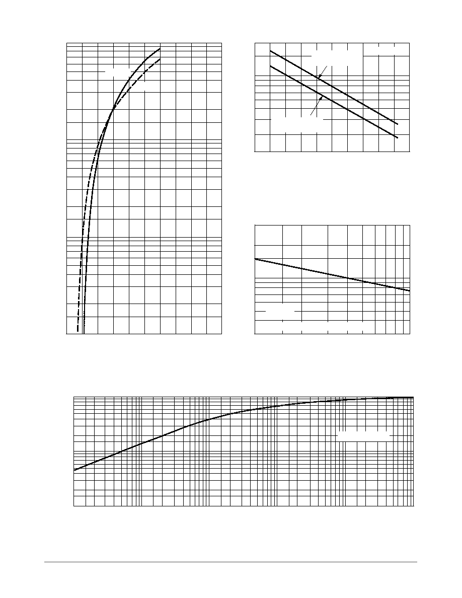
Figure 1. RMS Current Derating
Figure 2. OnşState Power Dissipation
Figure 3. Typical Gate Trigger Voltage
Figure 4. Typical Gate Trigger Current
130
120
110
100
90
80
0
2
4
6
8
10
12
14
16
IT(RMS), RMS ONşSTATE CURRENT (AMP)
T
C
, CASE
TEMPERA
TURE
(
C
)
░
= 30
░
= 180
░
= 60
░
= 90
░
dc
TJ
125
░
20
16
12
8
4
0
0
2
4
6
8
10
12
14
16
IT(RMS), ONşSTATE CURRENT (AMP)
30
░
= 180
░
dc
TJ
125
░
60
░
90
░
120
░
P
AV
,
A
VERAGE POWER (W
A
TTS)
= CONDUCTION ANGLE
= CONDUCTION ANGLE
1.8
1.6
1.4
1.2
1.0
0.4
ş60
ş40
ş20
0
20
40
60
80
100
TJ, JUNCTION TEMPERATURE (
░
C)
1
QUADRANT 4
0.8
0.6
120
140
2
3
QUADRANTS
OFFşSTATE VOLTAGE = 12 V
V
GT
, GA
TE
TRIGGER
VOL
T
AGE
(VOL
TS)
50
30
20
10
7.0
5.0
ş60
ş40
ş20
0
20
40
60
80
100
TJ, JUNCTION TEMPERATURE (
░
C)
1
120
140
2
3
QUADRANT
OFFşSTATE VOLTAGE = 12 V
4
I GT
, GA
TE
TRIGGER
CURRENT
(mA)
MAC15 Series
http://onsemi.com
5
100
70
50
30
20
0.4
0.8
1.2
1.6
2
2.4
2.8
3.2
3.6
vTM, INSTANTANEOUS ONşSTATE VOLTAGE (VOLTS)
TJ = 25
░
C
4
4.4
10
7
5
3
2
1
0.7
0.5
0.3
0.2
0.1
i TM
, INST
ANT
ANEOUS
FOR
W
ARD
CURRENT
(AMP)
125
░
C
20
10
7.0
5.0
3.0
2.0
ş60
ş40
ş20
0
20
40
60
80
100
TJ, JUNCTION TEMPERATURE (
░
C)
120
140
GATE OPEN
300
200
100
70
50
30
1
2
3
5
NUMBER OF CYCLES
7
10
Surge is preceded and followed by rated current
MAIN TERMINAL #1
POSITIVE
MAIN TERMINAL #2
POSITIVE
TC = 80
░
C
T
f = 60 Hz
T SM
, PEAK SURGE CURRENT
(AMP)
I H
, HOLDING CURRENT
(mA)
Figure 5. OnşState Characteristics
Figure 6. Typical Holding Current
Figure 7. Maximum NonşRepetitive
Surge Current
1
0.5
0.1
0.05
0.02
0.01
0.1
0.2
0.5
t, TIME (ms)
1
Z
JC(t) = r(t)
Ě
R
JC
0.2
2
5
10
20
50
100
200
500
1 k
2 k
5 k
10 k
r(t) TRANSIENT
THERMAL
RESIST
ANCE
(NORMALIZED)
Figure 8. Thermal Response
MAC15 Series
http://onsemi.com
6
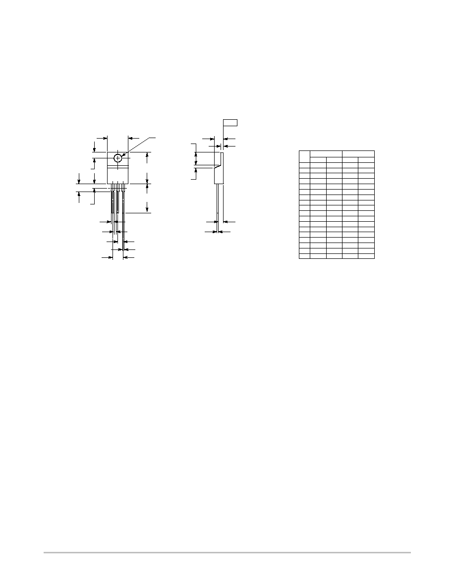
PACKAGE DIMENSIONS
STYLE 4:
PIN 1. MAIN TERMINAL 1
2. MAIN TERMINAL 2
3. GATE
4. MAIN TERMINAL 2
TOş220AB
CASE 221Aş07
ISSUE Z
NOTES:
1. DIMENSIONING AND TOLERANCING PER ANSI
Y14.5M, 1982.
2. CONTROLLING DIMENSION: INCH.
3. DIMENSION Z DEFINES A ZONE WHERE ALL
BODY AND LEAD IRREGULARITIES ARE
ALLOWED.
DIM
MIN
MAX
MIN
MAX
MILLIMETERS
INCHES
A
0.570
0.620
14.48
15.75
B
0.380
0.405
9.66
10.28
C
0.160
0.190
4.07
4.82
D
0.025
0.035
0.64
0.88
F
0.142
0.147
3.61
3.73
G
0.095
0.105
2.42
2.66
H
0.110
0.155
2.80
3.93
J
0.014
0.022
0.36
0.55
K
0.500
0.562
12.70
14.27
L
0.045
0.060
1.15
1.52
N
0.190
0.210
4.83
5.33
Q
0.100
0.120
2.54
3.04
R
0.080
0.110
2.04
2.79
S
0.045
0.055
1.15
1.39
T
0.235
0.255
5.97
6.47
U
0.000
0.050
0.00
1.27
V
0.045
şşş
1.15
şşş
Z
şşş
0.080
şşş
2.04
A
K
L
V
G
D
N
Z
H
Q
F
B
1
2
3
4
şTş
SEATING
PLANE
S
R
J
U
T
C

MAC15 Series
http://onsemi.com
7
Notes

MAC15 Series
http://onsemi.com
8
ON Semiconductor and are trademarks of Semiconductor Components Industries, LLC (SCILLC). SCILLC reserves the right to make changes
without further notice to any products herein. SCILLC makes no warranty, representation or guarantee regarding the suitability of its products for any particular
purpose, nor does SCILLC assume any liability arising out of the application or use of any product or circuit, and specifically disclaims any and all liability,
including without limitation special, consequential or incidental damages. "Typical" parameters which may be provided in SCILLC data sheets and/or
specifications can and do vary in different applications and actual performance may vary over time. All operating parameters, including "Typicals" must be
validated for each customer application by customer's technical experts. SCILLC does not convey any license under its patent rights nor the rights of others.
SCILLC products are not designed, intended, or authorized for use as components in systems intended for surgical implant into the body, or other applications
intended to support or sustain life, or for any other application in which the failure of the SCILLC product could create a situation where personal injury or
death may occur. Should Buyer purchase or use SCILLC products for any such unintended or unauthorized application, Buyer shall indemnify and hold
SCILLC and its officers, employees, subsidiaries, affiliates, and distributors harmless against all claims, costs, damages, and expenses, and reasonable
attorney fees arising out of, directly or indirectly, any claim of personal injury or death associated with such unintended or unauthorized use, even if such claim
alleges that SCILLC was negligent regarding the design or manufacture of the part. SCILLC is an Equal Opportunity/Affirmative Action Employer.
PUBLICATION ORDERING INFORMATION
CENTRAL/SOUTH AMERICA:
Spanish Phone: 303ş308ş7143 (MonşFri 8:00am to 5:00pm MST)
Email: ONlitşspanish@hibbertco.com
ASIA/PACIFIC: LDC for ON Semiconductor ş Asia Support
Phone: 303ş675ş2121 (TueşFri 9:00am to 1:00pm, Hong Kong Time)
Toll Free from Hong Kong & Singapore:
001ş800ş4422ş3781
Email: ONlitşasia@hibbertco.com
JAPAN: ON Semiconductor, Japan Customer Focus Center
4ş32ş1 NishişGotanda, Shinagawaşku, Tokyo, Japan 141ş8549
Phone: 81ş3ş5740ş2745
Email: r14525@onsemi.com
ON Semiconductor Website: http://onsemi.com
For additional information, please contact your local
Sales Representative.
MAC15A4/D
NORTH AMERICA Literature Fulfillment:
Literature Distribution Center for ON Semiconductor
P.O. Box 5163, Denver, Colorado 80217 USA
Phone: 303ş675ş2175 or 800ş344ş3860 Toll Free USA/Canada
Fax: 303ş675ş2176 or 800ş344ş3867 Toll Free USA/Canada
Email: ONlit@hibbertco.com
Fax Response Line: 303ş675ş2167 or 800ş344ş3810 Toll Free USA/Canada
N. American Technical Support: 800ş282ş9855 Toll Free USA/Canada
EUROPE: LDC for ON Semiconductor ş European Support
German Phone: (+1) 303ş308ş7140 (MşF 1:00pm to 5:00pm Munich Time)
Email: ONlitşgerman@hibbertco.com
French Phone: (+1) 303ş308ş7141 (MşF 1:00pm to 5:00pm Toulouse Time)
Email: ONlitşfrench@hibbertco.com
English Phone: (+1) 303ş308ş7142 (MşF 12:00pm to 5:00pm UK Time)
Email: ONlit@hibbertco.com
EUROPEAN TOLLşFREE ACCESS*: 00ş800ş4422ş3781
*Available from Germany, France, Italy, England, Ireland