©
Semiconductor Components Industries, LLC, 1999
October, 1999 Rev. 5
1
Publication Order Number:
LP2950/D
LP2950
Micropower Voltage
Regulators
The LP2950 and LP2951 are micropower voltage regulators that are
specifically designed to maintain proper regulation with an extremely
low inputtooutput voltage differential. These devices feature a very
low quiescent bias current of 75
µ
A and are capable of supplying
output currents in excess of 100 mA. Internal current and thermal
limiting protection is provided.
The LP2951 has three additional features. The first is the Error
Output that can be used to signal external circuitry of an out of
regulation condition, or as a microprocessor poweron reset. The
second feature allows the output voltage to be preset to 5.0 V, 3.3 V or
3.0 V output (depending on the version) or programmed from 1.25 V
to 29 V. It consists of a pinned out resistor divider along with direct
access to the Error Amplifier feedback input. The third feature is a
Shutdown input that allows a logic level signal to turnoff or turnon
the regulator output.
Due to the low inputtooutput voltage differential and bias current
specifications, these devices are ideally suited for battery powered
computer, consumer, and industrial equipment where an extension of
useful battery life is desirable. The LP2950 is available in the three
pin case 29 and DPAK packages, and the LP2951 is available in the
eight pin dualinline, SO8 and Micro8 surface mount packages.
The `A' suffix devices feature an initial output voltage tolerance
±
0.5%.
LP2950 and LP2951 Features:
·
Low Quiescent Bias Current of 75
µ
A
·
Low InputtoOutput Voltage Differential of 50 mV at 100
µ
A and
380 mV at 100 mA
·
5.0 V, 3.3 V or 3.0 V
±
0.5% Allows Use as a Regulator or Reference
·
Extremely Tight Line and Load Regulation
·
Requires Only a 1.0
µ
F Output Capacitor for Stability
·
Internal Current and Thermal Limiting
LP2951 Additional Features:
·
Error Output Signals an Out of Regulation Condition
·
Output Programmable from 1.25 V to 29 V
·
Logic Level Shutdown Input
(See Following Page for Device Information.)
TO92
Z SUFFIX
CASE 29
http://onsemi.com
See detailed ordering and shipping information in the package
dimensions section on page 13 of this data sheet.
ORDERING INFORMATION
PIN CONNECTIONS
2
3
1
Pin: 1. Output
2. Ground
3. Input
DPAK
DT SUFFIX
CASE 369A
3
1
Heatsink surface (shown as terminal 4 in
case outline drawing) is connected to Pin 2.
1
2
3
(Top View)
Pin: 1. Input
2. Ground
3. Output
8
1
8
1
8
1
PIN CONNECTIONS
1
8
7
6
5
2
3
4
(Top View)
Output
Sense
Shutdown
Input
Feedback
Error Output
VO Tap
Gnd
SO8
D SUFFIX
CASE 751
N SUFFIX
CASE 626
Micro8
DM SUFFIX
CASE 846A
LP2950
http://onsemi.com
2
DEVICE INFORMATION
Output Voltage
Operating Junction
Package
3.0V
3.3V
5.0V
Adjustable
Operating Junction
Temperature Range
TO92
Suffix Z
LP2950CZ3.0
LP2950ACZ3.0
LP2950CZ3.3
LP2950ACZ3.3
LP2950CZ5.0
LP2950ACZ5.0
Not
Available
TJ = 40
°
to +125
°
C
DPAK
Suffix DT
LP2950CDT3.0
LP2950ACDT3.0
LP2950CDT3.3
LP2950ACDT3.3
LP2950CDT5.0
LP2950ACDT5.0
Not
Available
TJ = 40
°
to +125
°
C
SO8
Suffix D
LP2951CD3.0
LP2951ACD3.0
LP2951CD3.3
LP2951ACD3.3
LP2951CD
LP2951ACD
LP2951CD
LP2951ACD
TJ = 40
°
to +125
°
C
Micro8
Suffix DM
LP2951CDM3.0
LP2951ACDM3.0
LP2951CDM3.3
LP2951ACDM3.3
LP2951CDM
LP2951ACDM
LP2951CDM
LP2951ACDM
TJ = 40
°
to +125
°
C
DIP8
Suffix N
LP2951CN3.0
LP2951ACN3.0
LP2951CN3.3
LP2951ACN3.3
LP2951CN
LP2951ACN
LP2951CN
LP2951ACN
TJ = 40
°
to +125
°
C
LP2950Cxxx / LP2951Cxxxx
1% Output Voltage Precision at TJ = 25
°
C
LP2950ACxxx / LP2951ACxxxx
0.5% Output Voltage Precision at TJ = 25
°
C
From
CMOS/TTL
3
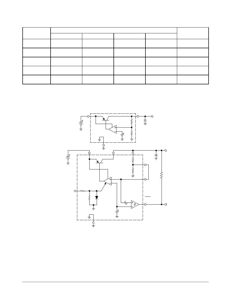
Representative Block Diagrams
This device contains 34 active transistors.
LP2950CZ5.0
Battery or
Unregulated DC
Gnd
2
Output
5.0 V/100 mA
1
Input
3
1.23 V
Reference
Error Amplifier
182 k
60 k
1.0
µ
F
Gnd
4
182 k
60 k
1.23 V
Reference
1.0
µ
F
LP2951CD or CN
Error
Amplifier
Battery or
Unregulated DC
Shutdown
Error
Output
5
VO Tap
Feedback
6
7
Input
8
Output
1
Sense
2
5.0 V/100 mA
330 k
To CMOS/TTL
75 mV/
60 mV
Error Detection
Comparator
50 k
60 k

LP2950
http://onsemi.com
3
MAXIMUM RATINGS
(TA = 25
°
C, unless otherwise noted.)
Rating
Symbol
Value
Unit
ÁÁÁÁÁÁÁÁÁÁÁÁÁÁÁÁÁÁÁ
ÁÁÁÁÁÁÁÁÁÁÁÁÁÁÁÁÁÁÁ
Input Voltage
ÁÁÁÁÁÁ
ÁÁÁÁÁÁ
VCC
ÁÁÁÁÁÁÁÁ
ÁÁÁÁÁÁÁÁ
30
ÁÁÁ
ÁÁÁ
Vdc
ÁÁÁÁÁÁÁÁÁÁÁÁÁÁÁÁÁÁÁ
ÁÁÁÁÁÁÁÁÁÁÁÁÁÁÁÁÁÁÁ
Power Dissipation and Thermal Characteristics
ÁÁÁÁÁÁ
ÁÁÁÁÁÁ
ÁÁÁÁÁÁÁÁ
ÁÁÁÁÁÁÁÁ
ÁÁÁ
ÁÁÁ
Maximum Power Dissipation
PD
Internally Limited
W
Case 751(SO8) D Suffix
Thermal Resistance, JunctiontoAmbient
R
JA
180
°
C/W
Thermal Resistance, JunctiontoCase
R
JC
45
°
C/W
Case 369A (DPAK) DT Suffix [Note 1]
Thermal Resistance, JunctiontoAmbient
R
JA
92
°
C/W
Thermal Resistance, JunctiontoCase
R
JC
6.0
°
C/W
Case 29 (TO226AA/TO92) Z Suffix
Thermal Resistance, JunctiontoAmbient
R
JA
160
°
C/W
Thermal Resistance, JunctiontoCase
R
JC
83
°
C/W
Case 626 N Suffix
Thermal Resistance, JunctiontoAmbient
R
JA
105
°
C/W
Case 846A (Micro8) DM Suffix
Thermal Resistance, JunctiontoAmbient
R
JA
240
°
C/W
ÁÁÁÁÁÁÁÁÁÁÁÁÁÁÁÁÁÁÁ
ÁÁÁÁÁÁÁÁÁÁÁÁÁÁÁÁÁÁÁ
Feedback Input Voltage
ÁÁÁÁÁÁ
ÁÁÁÁÁÁ
Vfb
ÁÁÁÁÁÁÁÁ
ÁÁÁÁÁÁÁÁ
1.5 to +30
ÁÁÁ
ÁÁÁ
Vdc
ÁÁÁÁÁÁÁÁÁÁÁÁÁÁÁÁÁÁÁ
ÁÁÁÁÁÁÁÁÁÁÁÁÁÁÁÁÁÁÁ
Shutdown Input Voltage
ÁÁÁÁÁÁ
ÁÁÁÁÁÁ
Vsd
ÁÁÁÁÁÁÁÁ
ÁÁÁÁÁÁÁÁ
0.3 to +30
ÁÁÁ
ÁÁÁ
Vdc
ÁÁÁÁÁÁÁÁÁÁÁÁÁÁÁÁÁÁÁ
ÁÁÁÁÁÁÁÁÁÁÁÁÁÁÁÁÁÁÁ
Error Comparator Output Voltage
ÁÁÁÁÁÁ
ÁÁÁÁÁÁ
Verr
ÁÁÁÁÁÁÁÁ
ÁÁÁÁÁÁÁÁ
0.3 to +30
ÁÁÁ
ÁÁÁ
Vdc
ÁÁÁÁÁÁÁÁÁÁÁÁÁÁÁÁÁÁÁ
ÁÁÁÁÁÁÁÁÁÁÁÁÁÁÁÁÁÁÁ
Operating Junction Temperature
ÁÁÁÁÁÁ
ÁÁÁÁÁÁ
TJ
ÁÁÁÁÁÁÁÁ
ÁÁÁÁÁÁÁÁ
40 to +125
ÁÁÁ
ÁÁÁ
°
C
ÁÁÁÁÁÁÁÁÁÁÁÁÁÁÁÁÁÁÁ
ÁÁÁÁÁÁÁÁÁÁÁÁÁÁÁÁÁÁÁ
Storage Temperature Range
ÁÁÁÁÁÁ
ÁÁÁÁÁÁ
Tstg
ÁÁÁÁÁÁÁÁ
ÁÁÁÁÁÁÁÁ
65 to +150
ÁÁÁ
ÁÁÁ
°
C
NOTE:
1. The JunctiontoAmbient Thermal Resistance is determined by PC board copper area per Figure 26.
2. ESD data available upon request.
ELECTRICAL CHARACTERISTICS
(Vin = VO + 1.0 V, IO = 100
µ
A, CO = 1.0
µ
F, TJ = 25
°
C [Note 1], unless
otherwise noted.)
Characteristic
Symbol
Min
Typ
Max
Unit
Output Voltage, 5.0 V Versions
VO
V
Vin = 6.0 V, IO = 100
µ
A, TJ = 25
°
C
LP2950C5.0/LP2951C
4.950
5.000
5.050
LP2950AC5.0/LP2951AC
4.975
5.000
5.025
TJ = 40 to +125
°
C
LP2950C5.0/LP2951C
4.900
5.100
LP2950AC5.0/LP2951AC
4.940
5.060
Vin = 6.0 to 30 V, IO = 100
µ
A to 100 mA, TJ = 40 to +125
°
C
LP2950C5.0/LP2951C
4.880
5.120
LP2950AC5.0/LP2951AC
4.925
5.075
Output Voltage, 3.3 V Versions
VO
V
Vin = 4.3 V, IO = 100
µ
A, TJ = 25
°
C
LP2950C3.3/LP2951C3.3
3.267
3.300
3.333
LP2950AC3.3/LP2951AC3.3
3.284
3.300
3.317
TJ = 40 to +125
°
C
LP2950C3.3/LP2951C3.3
3.234
3.366
LP2950AC3.3/LP2951AC3.3
3.260
3.340
Vin = 4.3 to 30 V, IO = 100
µ
A to 100 mA, TJ = 40 to +125
°
C
LP2950C3.3/LP2951C3.3
3.221
3.379
LP2950AC3.3/LP2951AC3.3
3.254
3.346
Output Voltage, 3.0 V Versions
VO
V
Vin = 4.0 V, IO = 100
µ
A, TJ = 25
°
C
LP2950C3.0/LP2951C3.0
2.970
3.000
3.030
LP2950AC3.0/LP2951AC3.0
2.985
3.000
3.015
TJ = 40 to +125
°
C
LP2950C3.0/LP2951C3.0
2.940
3.060
LP2950AC3.0/LP2951AC3.0
2.964
3.036
Vin = 4.0 to 30 V, IO = 100
µ
A to 100 mA, TJ = 40 to +125
°
C
LP2950C3.0/LP2951C3.0
2.928
3.072
LP2950AC3.0/LP2951AC3.0
2.958
3.042

LP2950
http://onsemi.com
4
ELECTRICAL CHARACTERISTICS (continued)
(Vin = VO + 1.0 V, IO = 100
µ
A, CO = 1.0
µ
F, TJ = 25
°
C [Note 1], unless
otherwise noted.)
Characteristic
Unit
Max
Typ
Min
Symbol
Line Regulation (Vin = VO(nom) +1.0 V to 30 V) [Note 2]
Regline
%
LP2950CXX/LP2951C/LP2951CXX
0.08
0.20
LP2950ACXX/LP2951AC/LP2951ACXX
0.04
0.10
Load Regulation (IO = 100
µ
A to 100 mA)
Regload
%
LP2950CXX/LP2951C/LP2951CXX
0.13
0.20
LP2950ACXX/LP2951AC/LP2951ACXX
0.05
0.10
Dropout Voltage
VI VO
mV
IO = 100
µ
A
30
80
IO = 100 mA
350
450
Supply Bias Current
ICC
IO = 100
µ
A
93
120
µ
A
IO = 100 mA
4.0
12
mA
Dropout Supply Bias Current (Vin = VO(nom) 0.5 V,
IO = 100
µ
A) [Note 2]
ICCdropout
110
170
µ
A
Current Limit (VO Shorted to Ground)
ILimit
220
300
mA
Thermal Regulation
Regthermal
0.05
0.20
%/W
Output Noise Voltage (10 Hz to 100 kHz) [Note 3]
Vn
µ
Vrms
CL = 1.0
µ
F
126
CL = 100
µ
F
56
LP2951A/LP2951AC ONLY
Reference Voltage (TJ = 25
°
C)
Vref
V
LP2951C/LP2951CXX
1.210
1.235
1.260
LP2951AC/LP2951ACXX
1.220
1.235
1.250
Reference Voltage (TJ = 40 to +125
°
C)
Vref
V
LP2951C/LP2951CXX
1.200
1.270
LP2951AC/LP2951ACXX
1.200
1.260
Reference Voltage (TJ = 40 to +125
°
C)
Vref
V
IO = 100
µ
A to 100 mA, Vin = 23 to 30 V
LP2951C/LP2951CXX
1.185
1.285
LP2951AC/LP2951ACXX
1.190
1.270
Feedback Pin Bias Current
IFB
15
40
nA
ERROR COMPARATOR
Output Leakage Current (VOH = 30 V)
Ilkg
0.01
1.0
µ
A
Output Low Voltage (Vin = 4.5 V, IOL = 400
µ
A)
VOL
150
250
mV
Upper Threshold Voltage (Vin = 6.0 V)
Vthu
40
45
mV
Lower Threshold Voltage (Vin = 6.0 V)
Vthl
60
95
mV
Hysteresis (Vin = 6.0 V)
Vhy
15
mV
SHUTDOWN INPUT
Input Logic Voltage
Vshtdn
V
Logic "0" (Regulator "On")
0
0.7
Logic "1" (Regulator "Off")
2.0
30
Shutdown Pin Input Current
Ishtdn
µ
A
Vshtdn = 2.4 V
35
50
Vshtdn = 30 V
450
600
Regulator Output Current in Shutdown Mode
Ioff
3.0
10
µ
A
(Vin = 30 V, Vshtdn = 2.0 V, VO = 0, Pin 6 Connected to Pin 7)
NOTES: 1. Low duty pulse techniques are used during test to maintain junction temperature as close to ambient as possible.
2. VO(nom) is the part number voltage option.
3.
Noise tests on the LP2951 are made with a 0.01
µ
F capacitor connected across Pins 7 and 1.

LP2950
http://onsemi.com
5
DEFINITIONS
Dropout Voltage The input/output voltage differential
at which the regulator output no longer maintains regulation
against further reductions in input voltage. Measured when
the output drops 100 mV below its nominal value (which is
measured at 1.0 V differential), dropout voltage is affected
by junction temperature, load current and minimum input
supply requirements.
Line Regulation The change in output voltage for a
change in input voltage. The measurement is made under
conditions of low dissipation or by using pulse techniques
such that average chip temperature is not significantly
affected.
Load Regulation The change in output voltage for a
change in load current at constant chip temperature.
Maximum Power Dissipation The maximum total
device dissipation for which the regulator will operate
within specifications.
Bias Current Current which is used to operate the
regulator chip and is not delivered to the load.
Output Noise Voltage The rms ac voltage at the output,
with constant load and no input ripple, measured over a
specified frequency range.
Leakage Current Current drawn through a bipolar
transistor collectorbase junction, under a specified
collector voltage, when the transistor is "off".
Upper Threshold Voltage Voltage applied to the
comparator input terminal, below the reference voltage
which is applied to the other comparator input terminal,
which causes the comparator output to change state from a
logic "0" to "1".
Lower Threshold Voltage Voltage applied to the
comparator input terminal, below the reference voltage
which is applied to the other comparator input terminal,
which causes the comparator output to change state from a
logic "1" to "0".
Hysteresis The difference between Lower Threshold
voltage and Upper Threshold voltage.
Figure 1. Quiescent Current
, OUTPUT
VOL
T
AGE
(V)
V
out
, OUTPUT
VOL
T
AGE
(V)
V
out
50
5.00
0
6.0
0
250
0.1
10
TA, AMBIENT TEMPERATURE (
°
C)
Vin, INPUT VOLTAGE (V)
B
IA
S
C
U
RRE
N
T
(
A)
µ
Vin, INPUT VOLTAGE (V)
LP
29
5
0
/LP
29
51
B
IA
S
C
U
RRE
N
T
(mA)
IL, LOAD CURRENT (mA)
Figure 2. Dropout Characteristics
Figure 3. Input Current
Figure 4. Output Voltage versus Temperature
1.0
10
100
1.0
2.0
3.0
4.0
5.0
6.0
5.0
10
15
20
25
0
50
100
150
1.0
0.1
0.01
5.0
4.0
3.0
2.0
1.0
0
4.99
4.98
4.97
4.96
4.95
200
150
100
50
0
RL = 50 k
RL = 50
0.1 mA Load Current
No Load
LP2951C
TA = 25
°
C
LP2951C
200