
©
Semiconductor Components Industries, LLC, 2002
August, 2002 Rev. 11
1
Publication Order Number:
LM358/D
LM358, LM258, LM2904,
LM2904A, LM2904V,
NCV2904
Single Supply Dual
Operational Amplifiers
Utilizing the circuit designs perfected for Quad Operational
Amplifiers, these dual operational amplifiers feature low power drain,
a common mode input voltage range extending to ground/V
EE
, and
single supply or split supply operation. The LM358 series is
equivalent to onehalf of an LM324.
These amplifiers have several distinct advantages over standard
operational amplifier types in single supply applications. They can
operate at supply voltages as low as 3.0 V or as high as 32 V, with
quiescent currents about onefifth of those associated with the
MC1741 (on a per amplifier basis). The common mode input range
includes the negative supply, thereby eliminating the necessity for
external biasing components in many applications. The output voltage
range also includes the negative power supply voltage.
·
Short Circuit Protected Outputs
·
True Differential Input Stage
·
Single Supply Operation: 3.0 V to 32 V (LM258/LM358)
3.0 V to 26 V (LM2904, A, V)
·
Low Input Bias Currents
·
Internally Compensated
·
Common Mode Range Extends to Negative Supply
·
Single and Split Supply Operation
·
ESD Clamps on the Inputs Increase Ruggedness of the Device
without Affecting Operation
PDIP8
N, AN, VN SUFFIX
CASE 626
1
8
SO8
D, VD SUFFIX
CASE 751
1
8
PIN CONNECTIONS
V
EE
/Gnd
Inputs A
Inputs B
Output B
Output A
V
CC
+
+
1
2
3
4
8
7
6
5
(Top View)
See general marking information in the device marking
section on page 11 of this data sheet.
DEVICE MARKING INFORMATION
See detailed ordering and shipping information in the package
dimensions section on page 10 of this data sheet.
ORDERING INFORMATION
Micro8
t
DMR2 SUFFIX
CASE 846A
1
8
http://onsemi.com
LM358, LM258, LM2904, LM2904A, LM2904V, NCV2904
http://onsemi.com
2
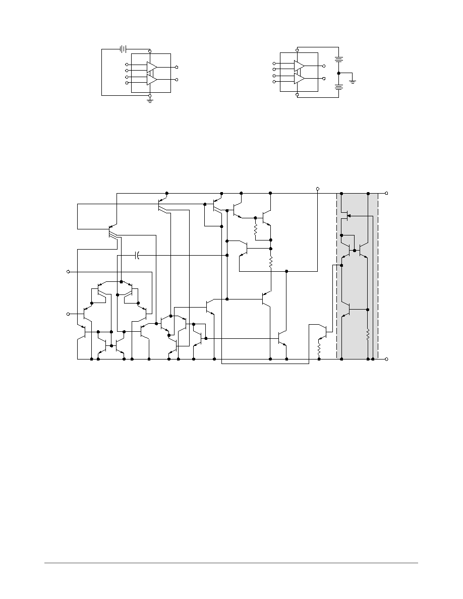
Single Supply
Split Supplies
V
CC
V
EE
/Gnd
3.0 V to V
CC(max)
1
2
V
CC
1
2
V
EE
1.5 V to V
CC(max)
1.5 V to V
EE(max)
Output
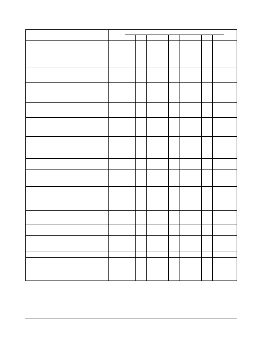
Bias Circuitry
Common to Both
Amplifiers
V
CC
V
EE
/Gnd
Inputs
Q2
Q3
Q4
Q5
Q26
Q7
Q8
Q6
Q9
Q11
Q10
Q1
2.4 k
Q25
Q22
40 k
Q13
Q14
Q15
Q16
Q19
5.0 pF
Q18
Q17
Q20
Q21
2.0 k
Q24
Q23
Q12
25
Figure 1.
Figure 2. Representative Schematic Diagram
(OneHalf of Circuit Shown)

LM358, LM258, LM2904, LM2904A, LM2904V, NCV2904
http://onsemi.com
3
MAXIMUM RATINGS
(T
A
= +25
°
C, unless otherwise noted.)
Rating
Symbol
LM258
LM358
LM2904, LM2904A
LM2904V, NCV2904
Unit
Power Supply Voltages
Vdc
Single Supply
V
CC
32
26
Split Supplies
V
CC
, V
EE
±
16
±
13
Input Differential Voltage Range (Note 1)
V
IDR
±
32
±
26
Vdc
Input Common Mode Voltage Range (Note 2)
V
ICR
0.3 to 32
0.3 to 26
Vdc
Output Short Circuit Duration
t
SC
Continuous
Junction Temperature
T
J
150
°
C
Thermal Resistance, JunctiontoAir (Note 3)
R
q
JA
238
°
C/W
Storage Temperature Range
T
stg
55 to +125
°
C
ESD Tolerance Human Body Model (Note 4)
2000
V
Operating Ambient Temperature Range
T
A
°
C
LM258
25 to +85
LM358
0 to +70
LM2904/LM2904A
40 to +105
LM2904V, NCV2904 (Note 5)
40 to +125
1. Split Power Supplies.
2. For Supply Voltages less than 32 V for the LM258/358 and 26 V for the LM2904, A, V, the absolute maximum input voltage is equal to the
supply voltage.
3. R
q
JA
for Case 846A.
4. ESD data available upon request.
5.
NCV2904 is qualified for automotive use.

LM358, LM258, LM2904, LM2904A, LM2904V, NCV2904
http://onsemi.com
4
ELECTRICAL CHARACTERISTICS
(V
CC
= 5.0 V, V
EE
= Gnd, T
A
= 25
°
C, unless otherwise noted.)
LM258
LM358
Characteristic
Symbol
Min
Typ
Max
Min
Typ
Max
Unit
Input Offset Voltage
V
CC
= 5.0 V to 30 V (26 V for LM2904, V),
V
IC
= 0 V to V
CC
1.7 V, V
O
]
1.4 V, R
S
= 0
V
IO
mV
T
A
= 25
°
C
2.0
5.0
2.0
7.0
T
A
= T
high
(Note 6)
7.0
9.0
T
A
= T
low
(Note 6)
7.0
9.0
Average Temperature Coefficient of Input Offset
Voltage
V
IO
/
T
7.0
7.0
µ
V/
°
C
T
A
= T
high
to T
low
(Note 6)
Input Offset Current
I
IO
3.0
30
5.0
50
nA
T
A
= T
high
to T
low
(Note 6)
100
150
Input Bias Current
I
IB
45
150
45
250
T
A
= T
high
to T
low
(Note 6)
50
300
50
500
Average Temperature Coefficient of Input Offset
Current
I
IO
/
T
10
10
pA/
°
C
T
A
= T
high
to T
low
(Note 6)
Input Common Mode Voltage Range (Note 7),
V
CC
= 30 V
(26 V for LM2904, V)
V
ICR
0
28.3
0
28.3
V
V
CC
= 30 V (26 V for LM2904, V),
T
A
= T
high
to T
low
0
28
0
28
Differential Input Voltage Range
V
IDR
V
CC
V
CC
V
Large Signal Open Loop Voltage Gain
A
VOL
V/mV
R
L
= 2.0 k
, V
CC
= 15 V, For Large V
O
Swing,
50
100
25
100
T
A
= T
high
to T
low
(Note 6)
25
15
Channel Separation
CS
120
120
dB
1.0 kHz
f
20 kHz, Input Referenced
Common Mode Rejection
CMR
70
85
65
70
dB
R
S
10 k
Power Supply Rejection
PSR
65
100
65
100
dB
Output VoltageHigh Limit
T
A
= T
high
to T
low
(Note 6)
V
OH
V
V
CC
= 5.0 V, R
L
= 2.0 k
, T
A
= 25
°
C
3.3
3.5
3.3
3.5
V
CC
= 30 V (26 V for LM2904, V), R
L
= 2.0 k
26
26
V
CC
= 30 V (26 V for LM2904, V), R
L
= 10 k
27
28
27
28
Output VoltageLow Limit
V
OL
5.0
20
5.0
20
mV
V
CC
= 5.0 V, R
L
= 10 k
,
T
A
= T
high
to T
low
(Note 6)
Output Source Current
I
O +
20
40
20
40
mA
V
ID
= +1.0 V, V
CC
= 15 V
Output Sink Current
I
O
V
ID
= 1.0 V, V
CC
= 15 V
10
20
10
20
mA
V
ID
= 1.0 V, V
O
= 200 mV
12
50
12
50
µ
A
Output Short Circuit to Ground (Note 8)
I
SC
40
60
40
60
mA
Power Supply Current (Total Device)
T
A
= T
high
to T
low
(Note 6)
I
CC
mA
V
CC
= 30 V (26 V for LM2904, V), V
O
= 0 V, R
L
=
1.5
3.0
1.5
3.0
V
CC
= 5 V, V
O
= 0 V, R
L
=
0.7
1.2
0.7
1.2
6. LM258: T
low
= 25
°
C, T
high
= +85
°
C
LM358: T
low
= 0
°
C, T
high
= +70
°
C
LM2904/LM2904A: T
low
= 40
°
C, T
high
= +105
°
C
LM2904V & NCV2904: T
low
= 40
°
C, T
high
= +125
°
C
NCV2904 is qualified for automotive use.
7. The input common mode voltage or either input signal voltage should not be allowed to go negative by more than 0.3 V. The upper end of
the common mode voltage range is V
CC
1.7 V.
8. Short circuits from the output to V
CC
can cause excessive heating and eventual destruction. Destructive dissipation can result from
simultaneous shorts on all amplifiers.
LM358, LM258, LM2904, LM2904A, LM2904V, NCV2904
http://onsemi.com
5
ELECTRICAL CHARACTERISTICS
(V
CC
= 5.0 V, V
EE
= Gnd, T
A
= 25
°
C, unless otherwise noted.)
LM2904
LM2904A
LM2904V, NCV2904
Characteristic
Symbol
Min
Typ
Max
Min
Typ
Max
Min
Typ
Max
Unit
Input Offset Voltage
V
CC
= 5.0 V to 30 V (26 V for LM2904, V),
V
IC
= 0 V to V
CC
1.7 V, V
O
]
1.4 V, R
S
= 0
V
IO
mV
T
A
= 25
°
C
2.0
7.0
2.0
7.0
7.0
T
A
= T
high
(Note 9)
10
10
13
T
A
= T
low
(Note 9)
10
10
10
Average Temperature Coefficient of Input Offset
Voltage
V
IO
/
T
7.0
7.0
7.0
µ
V/
°
C
T
A
= T
high
to T
low
(Note 9)
Input Offset Current
I
IO
5.0
50
5.0
50
5.0
50
nA
T
A
= T
high
to T
low
(Note 9)
45
200
45
200
45
200
Input Bias Current
I
IB
45
250
45
100
45
250
T
A
= T
high
to T
low
(Note 9)
50
500
50
250
50
500
Average Temperature Coefficient of Input Offset
Current
I
IO
/
T
10
10
10
pA/
°
C
T
A
= T
high
to T
low
(Note 9)
Input Common Mode Voltage Range (Note 10),
V
CC
= 30 V (26 V for LM2904, V)
V
ICR
0
24.3
0
24.3
0
24.3
V
V
CC
= 30 V (26 V for LM2904, V),
T
A
= T
high
to T
low
0
24
0
24
0
24
Differential Input Voltage Range
V
IDR
V
CC
V
CC
V
CC
V
Large Signal Open Loop Voltage Gain
A
VOL
V/mV
R
L
= 2.0 k
, V
CC
= 15 V, For Large V
O
Swing,
25
100
25
100
25
100
T
A
= T
high
to T
low
(Note 9)
15
15
15
Channel Separation
CS
120
120
120
dB
1.0 kHz
f
20 kHz, Input Referenced
Common Mode Rejection
CMR
50
70
50
70
50
70
dB
R
S
10 k
Power Supply Rejection
PSR
50
100
50
100
50
100
dB
Output VoltageHigh Limit
T
A
= T
high
to T
low
(Note 9)
V
OH
V
V
CC
= 5.0 V, R
L
= 2.0 k
, T
A
= 25
°
C
3.3
3.5
3.3
3.5
3.3
3.5
V
CC
= 30 V (26 V for LM2904, V), R
L
= 2.0 k
22
22
22
V
CC
= 30 V (26 V for LM2904, V), R
L
= 10 k
23
24
23
24
23
24
Output VoltageLow Limit
V
OL
5.0
20
5.0
20
5.0
20
mV
V
CC
= 5.0 V, R
L
= 10 k
,
T
A
= T
high
to T
low
(Note 9)
Output Source Current
I
O +
20
40
20
40
20
40
mA
V
ID
= +1.0 V, V
CC
= 15 V
Output Sink Current
I
O
V
ID
= 1.0 V, V
CC
= 15 V
10
20
10
20
10
20
mA
V
ID
= 1.0 V, V
O
= 200 mV
µ
A
Output Short Circuit to Ground (Note 11)
I
SC
40
60
40
60
40
60
mA
Power Supply Current (Total Device)
T
A
= T
high
to T
low
(Note 9)
I
CC
mA
V
CC
= 30 V (26 V for LM2904, V), V
O
= 0 V,
R
L
=
1.5
3.0
1.5
3.0
1.5
3.0
V
CC
= 5 V, V
O
= 0 V, R
L
=
0.7
1.2
0.7
1.2
0.7
1.2
9. LM258: T
low
= 25
°
C, T
high
= +85
°
C
LM358: T
low
= 0
°
C, T
high
= +70
°
C
LM2904/LM2904A: T
low
= 40
°
C, T
high
= +105
°
C
LM2904V & NCV2904: T
low
= 40
°
C, T
high
= +125
°
C
NCV2904 is qualified for automotive use.
10. The input common mode voltage or either input signal voltage should not be allowed to go negative by more than 0.3 V. The upper end of
the common mode voltage range is V
CC
1.7 V.
11. Short circuits from the output to V
CC
can cause excessive heating and eventual destruction. Destructive dissipation can result from
simultaneous shorts on all amplifiers.