Äîêóìåíòàöèÿ è îïèñàíèÿ www.docs.chipfind.ru
©
Semiconductor Components Industries, LLC, 2004
January, 2004 - Rev. 3
1
Publication Order Number:
BC856BDW1T1/D
BC856BDW1T1,
BC857BDW1T1 Series,
BC858BDW1T1 Series
Preferred Devices
Dual General Purpose
Transistors
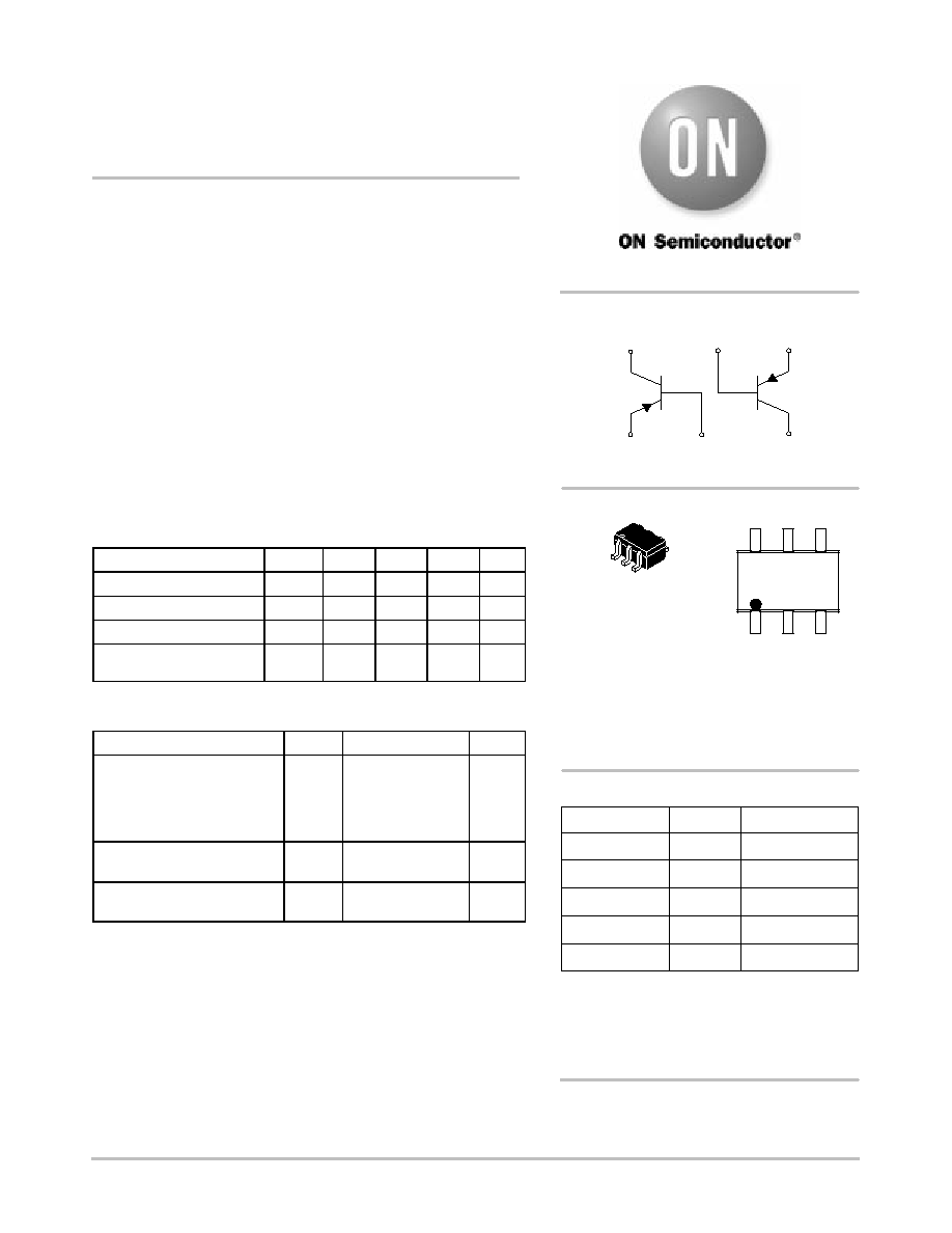
PNP Duals
These transistors are designed for general purpose amplifier
applications. They are housed in the SOT-363/SC-88 which is
designed for low power surface mount applications.
·
Device Marking:
BC856BDW1T1 = 3B
BC857BDW1T1 = 3F
BC857CDW1T1 = 3G
BC858BDW1T1 = 3K
BC858CDW1T1 = 3L
MAXIMUM RATINGS
Rating
Symbol
BC856
BC857
BC858
Unit
Collector - Emitter Voltage
V
CEO
-65
-45
-30
V
Collector - Base Voltage
V
CBO
-80
-50
-30
V
Emitter - Base Voltage
V
EBO
-5.0
-5.0
-5.0
V
Collector Current -
Continuous
I
C
-100
-100
-100
mAdc
THERMAL CHARACTERISTICS
Characteristic
Symbol
Max
Unit
Total Device Dissipation
Per Device
FR- 5 Board (Note 1)
T
A
= 25
°
C
Derate Above 25
°
C
P
D
380
250
3.0
mW
mW/
°
C
Thermal Resistance,
Junction to Ambient
R
q
JA
328
°
C/W
Junction and Storage
Temperature Range
T
J
, T
stg
- 55 to +150
°
C
1. FR-5 = 1.0 x 0.75 x 0.062 in
Device
Package
Shipping
ORDERING INFORMATION
BC857BDW1T1
SOT-363
SOT-363/SC-88
CASE 419B
Style 1
3000 Units/Reel
DEVICE MARKING
Preferred devices are recommended choices for future use
and best overall value.
BC857CDW1T1
SOT-363
3000 Units/Reel
BC858BDW1T1
SOT-363
3000 Units/Reel
BC858CDW1T1
SOT-363
3000 Units/Reel
3xm
See Table
Q
1
(1)
(2)
(3)
(4)
(5)
(6)
Q
2
1
2
3
6 5
4
BC856BDW1T1
SOT-363
3000 Units/Reel
3x = Specific Device Code
x
= B, F, G, K, L
M = Date Code
http://onsemi.com
For information on tape and reel specifications,
including part orientation and tape sizes, please
refer to our Tape and Reel Packaging Specifications
Brochure, BRD8011/D.
BC856BDW1T1, BC857BDW1T1 Series, BC858BDW1T1 Series
http://onsemi.com
2
ELECTRICAL CHARACTERISTICS
(T
A
= 25
°
C unless otherwise noted)
Characteristic
Symbol
Min
Typ
Max
Unit
OFF CHARACTERISTICS
Collector - Emitter Breakdown Voltage
(I
C
= -10 mA)
BC856 Series
BC857 Series
BC858 Series
V
(BR)CEO
-65
-45
-30
-
-
-
-
-
-
V
Collector - Emitter Breakdown Voltage
(I
C
= -10
m
A, V
EB
= 0)
BC856 Series
BC857B Only
BC858 Series
V
(BR)CES
-80
-50
-30
-
-
-
-
-
-
V
Collector - Base Breakdown Voltage
(I
C
= -10
m
A)
BC856 Series
BC857 Series
BC858 Series
V
(BR)CBO
-80
-50
-30
-
-
-
-
-
-
V
Emitter - Base Breakdown Voltage
(I
E
= -1.0
m
A)
BC856 Series
BC857 Series
BC858 Series
V
(BR)EBO
-5.0
-5.0
-5.0
-
-
-
-
-
-
V
Collector Cutoff Current (V
CB
= -30 V)
Collector Cutoff Current
(V
CB
= -30 V, T
A
= 150
°
C)
I
CBO
-
-
-
-
-15
-4.0
nA
m
A
ON CHARACTERISTICS
DC Current Gain
(I
C
= -10
m
A, V
CE
= -5.0 V)
BC856B, BC857B, BC858B
BC857C, BC858C
(I
C
= -2.0 mA, V
CE
= -5.0 V)
BC856B, BC857B, BC858B
BC857C, BC858C
h
FE
-
-
220
420
150
270
290
520
-
-
475
800
-
Collector - Emitter Saturation Voltage
(I
C
= -10 mA, I
B
= -0.5 mA)
(I
C
= -100 mA, I
B
= -5.0 mA)
V
CE(sat)
-
-
-
-
-0.3
-0.65
V
Base - Emitter Saturation Voltage
(I
C
= -10 mA, I
B
= -0.5 mA)
(I
C
= -100 mA, I
B
= -5.0 mA)
V
BE(sat)
-
-
-0.7
-0.9
-
-
V
Base - Emitter On Voltage
(I
C
= -2.0 mA, V
CE
= -5.0 V)
(I
C
= -10 mA, V
CE
= -5.0 V)
V
BE(on)
-0.6
-
-
-
-0.75
-0.82
V
SMALL-SIGNAL CHARACTERISTICS
Current - Gain - Bandwidth Product
(I
C
= -10 mA, V
CE
= -5.0 Vdc, f = 100 MHz)
f
T
100
-
-
MHz
Output Capacitance
(V
CB
= -10 V, f = 1.0 MHz)
C
ob
-
-
4.5
pF
Noise Figure
(I
C
= -0.2 mA, V
CE
= -5.0 Vdc, R
S
= 2.0 k
W
,
f = 1.0 kHz, BW = 200 Hz)
NF
-
-
10
dB
BC856BDW1T1, BC857BDW1T1 Series, BC858BDW1T1 Series
http://onsemi.com
3
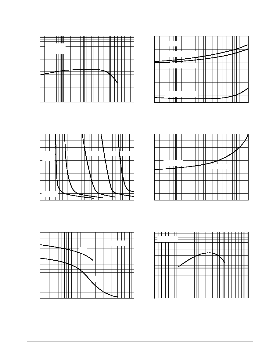
TYPICAL CHARACTERISTICS - BC856
Figure 1. DC Current Gain
I
C
, COLLECTOR CURRENT (mA)
Figure 2. "On" Voltage
I
C
, COLLECTOR CURRENT (mA)
-0.8
-1.0
-0.6
-0.2
-0.4
1.0
2.0
-0.1
-1.0
-10
-200
-0.2
0.2
0.5
-0.2
-1.0
-10
-200
T
J
= 25
°
C
V
BE(sat)
@ I
C
/I
B
= 10
V
CE(sat)
@ I
C
/I
B
= 10
V
BE
@ V
CE
= -5.0 V
Figure 3. Collector Saturation Region
I
B
, BASE CURRENT (mA)
Figure 4. Base-Emitter Temperature Coefficient
I
C
, COLLECTOR CURRENT (mA)
-1.0
-1.2
-1.6
-2.0
-0.02
-1.0
-10
0
-20
-0.1
-0.4
-0.8
V CE
, COLLECT
OR-EMITTER VOL
T
AGE (VOL
TS)
VB
,
TEMPERA
TURE COEFFICIENT
(mV/
C)
°
-0.2
-2.0
-10
-200
-1.0
T
J
= 25
°
C
I
C
=
-10 mA
h FE
, DC CURRENT
GAIN (NORMALIZED)
V
,
VOL
T
AGE (VOL
TS)
V
CE
= -5.0 V
T
A
= 25
°
C
0
-0.5
-2.0
-5.0
-20
-50 -100
-0.05
-0.2
-0.5
-2.0
-5.0
-100 mA
-20 mA
-1.4
-1.8
-2.2
-2.6
-3.0
-0.5
-5.0
-20
-50 -100
-55
°
C to 125
°
C
q
VB
for V
BE
-2.0 -5.0
-20
-50 -100
Figure 5. Capacitance
V
R
, REVERSE VOLTAGE (VOLTS)
40
Figure 6. Current-Gain - Bandwidth Product
I
C
, COLLECTOR CURRENT (mA)
-0.1 -0.2
-1.0
-50
2.0
-2.0
-10
-100
100
200
500
50
20
20
10
6.0
4.0
-1.0
-10
-100
V
CE
= -5.0 V
C, CAP
ACIT
ANCE (pF)
f, CURRENT-GAIN - BANDWIDTH PRODUCT T
-0.5
-5.0
-20
T
J
= 25
°
C
C
ob
C
ib
8.0
-50 mA
-200 mA
BC856BDW1T1, BC857BDW1T1 Series, BC858BDW1T1 Series
http://onsemi.com
4
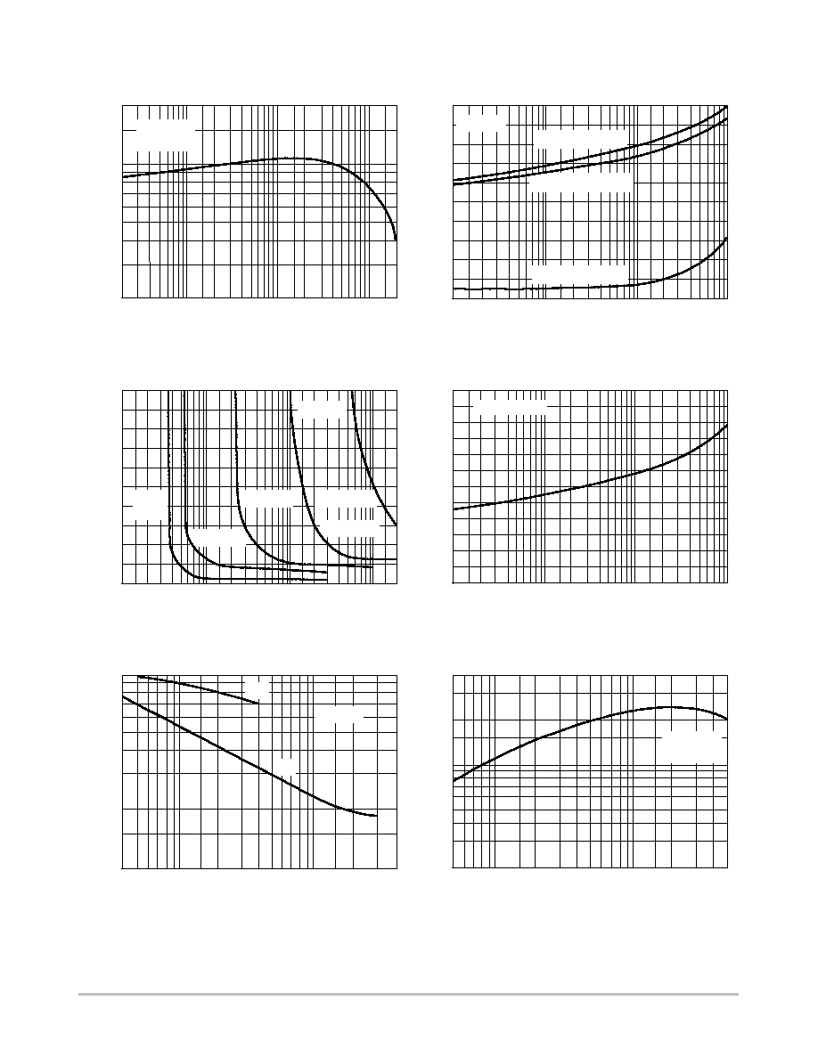
TYPICAL CHARACTERISTICS - BC857/BC858
Figure 7. Normalized DC Current Gain
I
C
, COLLECTOR CURRENT (mAdc)
2.0
Figure 8. "Saturation" and "On" Voltages
I
C
, COLLECTOR CURRENT (mAdc)
-0.2
0.2
Figure 9. Collector Saturation Region
I
B
, BASE CURRENT (mA)
Figure 10. Base-Emitter Temperature
Coefficient
I
C
, COLLECTOR CURRENT (mA)
-0.6
-0.7
-0.8
-0.9
-1.0
-0.5
0
-0.2
-0.4
-0.1
-0.3
1.6
1.2
2.0
2.8
2.4
-1.2
-1.6
-2.0
-0.02
-1.0
-10
0
-20
-0.1
-0.4
-0.8
h FE
, NORMALIZED DC CURRENT
GAIN
V
,
VOL
T
AGE (VOL
TS)
V CE
, COLLECT
OR-EMITTER VOL
T
AGE (V)
VB
,
TEMPERA
TURE COEFFICIENT
(mV/
C)
°
1.5
1.0
0.7
0.5
0.3
-0.2
-10
-100
-1.0
T
A
= 25
°
C
V
BE(sat)
@ I
C
/I
B
= 10
V
CE(sat)
@ I
C
/I
B
= 10
V
BE(on)
@ V
CE
= -10 V
V
CE
= -10 V
T
A
= 25
°
C
-55
°
C to +125
°
C
I
C
= -100 mA
I
C
= -20 mA
-0.5 -1.0 -2.0
-5.0 -10
-20
-50 -100 -200
-0.1 -0.2
-0.5 -1.0 -2.0
-5.0
-10 -20
-50 -100
I
C
= -200 mA
I
C
= -50 mA
I
C
=
-10 mA
Figure 11. Capacitances
V
R
, REVERSE VOLTAGE (VOLTS)
10
Figure 12. Current-Gain - Bandwidth Product
I
C
, COLLECTOR CURRENT (mAdc)
-0.4
1.0
80
100
200
300
400
60
20
40
30
7.0
5.0
3.0
2.0
-0.5
C, CAP
ACIT
ANCE (pF)
f, CURRENT-GAIN - BANDWIDTH PRODUCT
(MHz)
T
T
A
= 25
°
C
C
ob
C
ib
-0.6
-1.0
-2.0
-4.0 -6.0
-10
-20 -30 -40
150
-1.0
-2.0 -3.0
-5.0
-10
-20 -30
-50
V
CE
= -10 V
T
A
= 25
°
C
T
A
= 25
°
C
1.0
BC856BDW1T1, BC857BDW1T1 Series, BC858BDW1T1 Series
http://onsemi.com
5
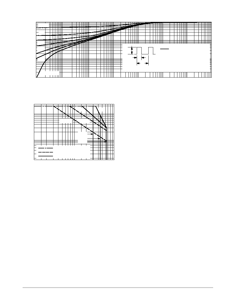
Figure 13. Thermal Response
Figure 14. Active Region Safe Operating Area
V
CE
, COLLECTOR-EMITTER VOLTAGE (V)
-200
-1.0
I C
, COLLECT
OR CURRENT
(mA)
T
A
= 25
°
C
BONDING WIRE LIMIT
THERMAL LIMIT
SECOND BREAKDOWN LIMIT
3 ms
T
J
= 25
°
C
-100
-50
-10
-5.0
-2.0
-5.0
-10
-30 -45 -65 -100
1 s
BC558
BC557
BC556
The safe operating area curves indicate I
C
-V
CE
limits
of the transistor that must be observed for reliable opera-
tion. Collector load lines for specific circuits must fall be-
low the limits indicated by the applicable curve.
The data of Figure 14 is based upon T
J(pk)
= 150
°
C; T
C
or T
A
is variable depending upon conditions. Pulse curves
are valid for duty cycles to 10% provided T
J(pk)
150
°
C.
T
J(pk)
may be calculated from the data in Figure 13. At high
case or ambient temperatures, thermal limitations will re-
duce the power that can be handled to values less than the
limitations imposed by the secondary breakdown.
t, TIME (ms)
1.0
r(t), TRANSIENT
THERMAL
1.0
0
RESIST
ANCE (NORMALIZED)
0.1
0.01
0.001
10
100
1.0 k
10 k
100 k
D = 0.5
0.2
0.1
0.05
SINGLE PULSE
Z
q
JA
(t) = r(t) R
q
JA
R
q
JA
= 328
°
C/W MAX
D CURVES APPLY FOR POWER
PULSE TRAIN SHOWN
READ TIME AT t
1
T
J(pk)
- T
C
= P
(pk)
R
q
JC
(t)
t
1
t
2
P
(pk)
DUTY CYCLE, D = t
1
/t
2
1.0 M
0.02
0.01
BC856BDW1T1, BC857BDW1T1 Series, BC858BDW1T1 Series
http://onsemi.com
6
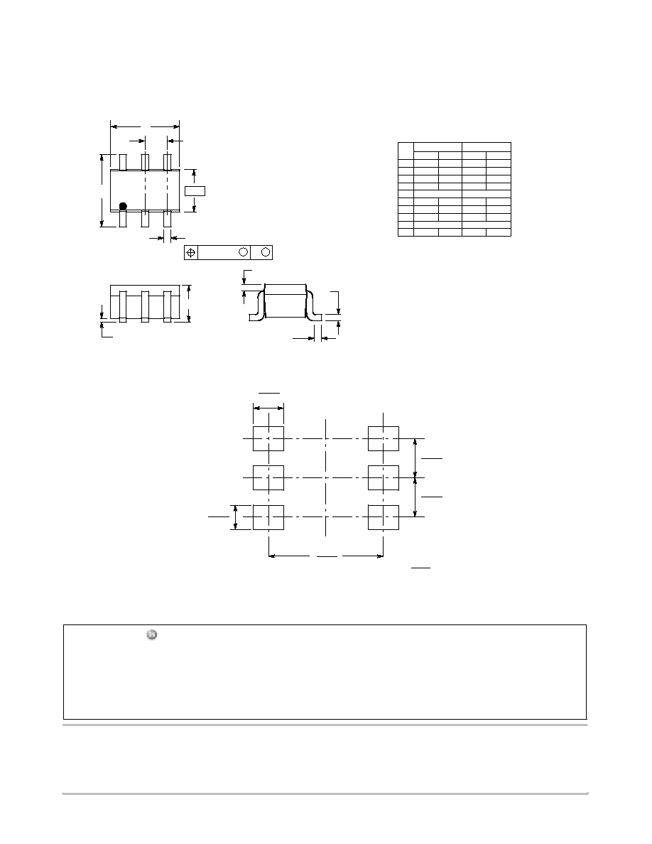
PACKAGE DIMENSIONS
SC-88 (SOT-363)
CASE 419B-02
ISSUE T
STYLE 1:
PIN 1. EMITTER 2
2. BASE 2
3. COLLECTOR 1
4. EMITTER 1
5. BASE 1
6. COLLECTOR 2
NOTES:
1. DIMENSIONING AND TOLERANCING PER ANSI
Y14.5M, 1982.
2. CONTROLLING DIMENSION: INCH.
3. 419B-01 OBSOLETE, NEW STANDARD 419B-02.
DIM
A
MIN
MAX
MIN
MAX
MILLIMETERS
1.80
2.20
0.071
0.087
INCHES
B
1.15
1.35
0.045
0.053
C
0.80
1.10
0.031
0.043
D
0.10
0.30
0.004
0.012
G
0.65 BSC
0.026 BSC
H
---
0.10
---
0.004
J
0.10
0.25
0.004
0.010
K
0.10
0.30
0.004
0.012
N
0.20 REF
0.008 REF
S
2.00
2.20
0.079
0.087
B
0.2 (0.008)
M
M
1
2
3
A
G
S
H
C
N
J
K
6
5
4
-B-
D
6 PL
SC-88/SC70-6
mm
inches
SCALE 20:1
0.65
0.025
0.65
0.025
0.50
0.0197
0.40
0.0157
1.9
0.0748
SOLDERING FOOTPRINT*
ON Semiconductor and are registered trademarks of Semiconductor Components Industries, LLC (SCILLC). SCILLC reserves the right to make changes without further notice
to any products herein. SCILLC makes no warranty, representation or guarantee regarding the suitability of its products for any particular purpose, nor does SCILLC assume any liability
arising out of the application or use of any product or circuit, and specifically disclaims any and all liability, including without limitation special, consequential or incidental damages.
"Typical" parameters which may be provided in SCILLC data sheets and/or specifications can and do vary in different applications and actual performance may vary over time. All
operating parameters, including "Typicals" must be validated for each customer application by customer's technical experts. SCILLC does not convey any license under its patent rights
nor the rights of others. SCILLC products are not designed, intended, or authorized for use as components in systems intended for surgical implant into the body, or other applications
intended to support or sustain life, or for any other application in which the failure of the SCILLC product could create a situation where personal injury or death may occur. Should
Buyer purchase or use SCILLC products for any such unintended or unauthorized application, Buyer shall indemnify and hold SCILLC and its officers, employees, subsidiaries, affiliates,
and distributors harmless against all claims, costs, damages, and expenses, and reasonable attorney fees arising out of, directly or indirectly, any claim of personal injury or death
associated with such unintended or unauthorized use, even if such claim alleges that SCILLC was negligent regarding the design or manufacture of the part. SCILLC is an Equal
Opportunity/Affirmative Action Employer. This literature is subject to all applicable copyright laws and is not for resale in any manner.
PUBLICATION ORDERING INFORMATION
N. American Technical Support: 800-282-9855 Toll Free
USA/Canada
Japan: ON Semiconductor, Japan Customer Focus Center
2-9-1 Kamimeguro, Meguro-ku, Tokyo, Japan 153-0051
Phone: 81-3-5773-3850
BC856BDW1T1/D
LITERATURE FULFILLMENT:
Literature Distribution Center for ON Semiconductor
P.O. Box 5163, Denver, Colorado 80217 USA
Phone: 303-675-2175 or 800-344-3860 Toll Free USA/Canada
Fax: 303-675-2176 or 800-344-3867 Toll Free USA/Canada
Email: orderlit@onsemi.com
ON Semiconductor Website: http://onsemi.com
Order Literature: http://www.onsemi.com/litorder
For additional information, please contact your
local Sales Representative.