®
Semiconductor Components Industries, LLC, 2004
March, 2004 - Rev. 8
1
Publication Order Number:
BAS40-04LT1/D
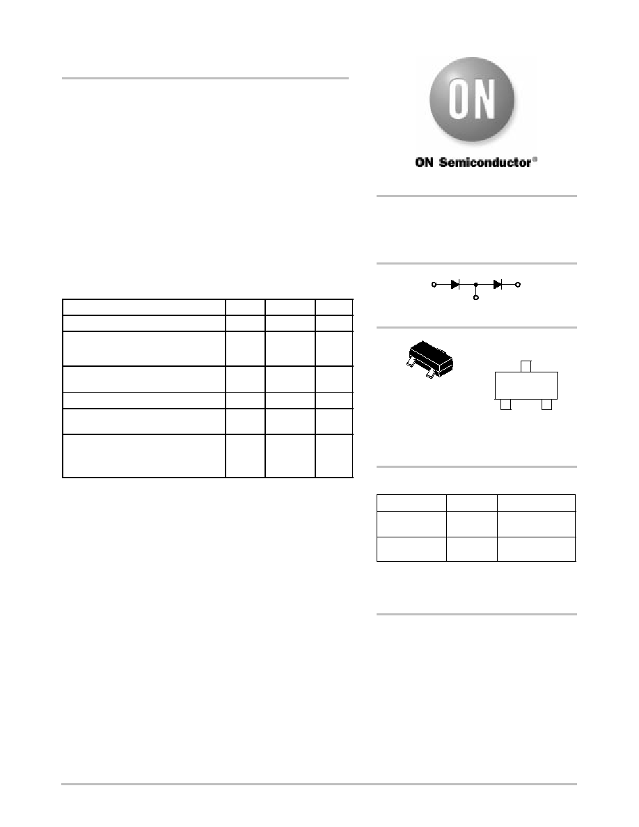
BAS40-04LT1
Preferred Device
Dual Series
Schottky Barrier Diode
These Schottky barrier diodes are designed for high speed switching
applications, circuit protection, and voltage clamping. Extremely low
forward voltage reduces conduction loss. Miniature surface mount
package is excellent for hand held and portable applications where
space is limited.
À
Extremely Fast Switching Speed
À
Low Forward Voltage
Features
À
Pb-Free Package is Available
MAXIMUM RATINGS
Rating
Symbol
Value
Unit
Reverse Voltage
V
R
40
V
Forward Power Dissipation
@ T
A
= 25
░
C
Derate above 25
░
C
P
F
225
1.8
mW
mW/
░
C
Operating Junction and Storage Temper-
ature Range
T
J,
T
stg
- 55 to
+150
░
C
Forward Continuous Current
I
FM
120
mA
Single Forward Current
t
v
1 s
t
v
10 ms
I
FSM
200
600
mA
Thermal Resistance
Junction-to-Ambient
R
q
JA
508
(Note 1)
311
(Note 2)
░
C/W
Maximum ratings are those values beyond which device damage can occur.
Maximum ratings applied to the device are individual stress limit values (not
normal operating conditions) and are not valid simultaneously. If these limits
are exceeded, device functional operation is not implied, damage may occur
and reliability may be affected.
1. FR-4 @ minimum pad.
2. FR-4 @ 1.0 x 1.0 in pad.
http://onsemi.com
Preferred devices are recommended choices for future use
and best overall value.
Device
Package
Shipping
ORDERING INFORMATION
BAS40-04LT1
SOT-23
3000/ Tape &
Reel
SOT-23 (TO-236AB)
CASE 318
Style 11
40 VOLTS
SCHOTTKY BARRIER DIODES
MARKING
DIAGRAM
CB
= Specific Device Code
D
= Date Code
1
2
3
CB D
ANODE
1
CATHODE
2
3
CATHODE/ANODE
BAS40-04LT1G
SOT-23
(Pb-Free)
3000/ Tape &
Reel
For information on tape and reel specifications,
including part orientation and tape sizes, please
refer to our Tape and Reel Packaging Specifications
Brochure, BRD8011/D.
BAS40-04LT1
http://onsemi.com
3
100
0
0.1
V
F
, FORWARD VOLTAGE (VOLTS)
0.2
0.3
0.4
0.5
10
1.0
0.1
85
░
C
10
0
V
R
, REVERSE VOLTAGE (VOLTS)
1.0
0.1
0.01
0.001
5.0
10
15
20
25
3.5
0
V
R
, REVERSE VOLTAGE (VOLTS)
3.0
1.0
0.5
0
C T
, CAP
ACIT
ANCE (pF)
5.0
10
15
40
I F
, FOR
W
ARD CURRENT
(mA)
Figure 1. Typical Forward Voltage
Figure 2. Reverse Current versus Reverse
Voltage
Figure 3. Typical Capacitance
-40
░
C
25
░
C
T
A
= 150
░
C
25
░
C
I R
, REVERSE CURRENT
(
Á
A)
0.8
-55
░
C
125
░
C
150
░
C
100
25
20
1.5
2.0
2.5
0.6
0.7
125
░
C
85
░
C
30
35
BAS40-04LT1
http://onsemi.com
4
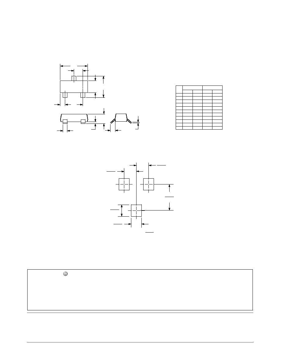
PACKAGE DIMENSIONS
CASE 318-08
ISSUE AH
SOT-23 (TO-236AB)
DIM
A
MIN
MAX
MIN
MAX
MILLIMETERS
0.1102 0.1197
2.80
3.04
INCHES
B 0.0472 0.0551
1.20
1.40
C 0.0385 0.0498
0.99
1.26
D 0.0140 0.0200
0.36
0.50
G 0.0670 0.0826
1.70
2.10
H 0.0040 0.0098
0.10
0.25
J 0.0034 0.0070
0.085
0.177
K 0.0180 0.0236
0.45
0.60
L 0.0350 0.0401
0.89
1.02
S 0.0830 0.0984
2.10
2.50
V 0.0177 0.0236
0.45
0.60
NOTES:
1. DIMENSIONING AND TOLERANCING PER ANSI
Y14.5M, 1982.
2. CONTROLLING DIMENSION: INCH.
3. MAXIUMUM LEAD THICKNESS INCLUDES LEAD
FINISH THICKNESS. MINIMUM LEAD THICKNESS
IS THE MINIMUM THICKNESS OF BASE
MATERIAL.
4. 318-01, -02, AND -06 OBSOLETE, NEW
STANDARD 318-09.
1
3
2
A
L
B
S
V
G
D
H
C
K
J
STYLE 11:
PIN 1. ANODE
2. CATHODE
3. CATHODE-ANODE
SOT-123
*For additional information on our Pb-Free strategy and soldering
details, please download the ON Semiconductor Soldering and
Mounting Techniques Reference Manual, SOLDERRM/D.
SOLDERING FOOTPRINT*
mm
inches
SCALE 10:1
0.8
0.031
0.9
0.035
0.95
0.037
0.95
0.037
2.0
0.079
ON Semiconductor and are registered trademarks of Semiconductor Components Industries, LLC (SCILLC). SCILLC reserves the right to make changes without further notice
to any products herein. SCILLC makes no warranty, representation or guarantee regarding the suitability of its products for any particular purpose, nor does SCILLC assume any liability
arising out of the application or use of any product or circuit, and specifically disclaims any and all liability, including without limitation special, consequential or incidental damages.
"Typical" parameters which may be provided in SCILLC data sheets and/or specifications can and do vary in different applications and actual performance may vary over time. All
operating parameters, including "Typicals" must be validated for each customer application by customer's technical experts. SCILLC does not convey any license under its patent rights
nor the rights of others. SCILLC products are not designed, intended, or authorized for use as components in systems intended for surgical implant into the body, or other applications
intended to support or sustain life, or for any other application in which the failure of the SCILLC product could create a situation where personal injury or death may occur. Should
Buyer purchase or use SCILLC products for any such unintended or unauthorized application, Buyer shall indemnify and hold SCILLC and its officers, employees, subsidiaries, affiliates,
and distributors harmless against all claims, costs, damages, and expenses, and reasonable attorney fees arising out of, directly or indirectly, any claim of personal injury or death
associated with such unintended or unauthorized use, even if such claim alleges that SCILLC was negligent regarding the design or manufacture of the part. SCILLC is an Equal
Opportunity/Affirmative Action Employer. This literature is subject to all applicable copyright laws and is not for resale in any manner.
PUBLICATION ORDERING INFORMATION
N. American Technical Support: 800-282-9855 Toll Free
USA/Canada
Japan: ON Semiconductor, Japan Customer Focus Center
2-9-1 Kamimeguro, Meguro-ku, Tokyo, Japan 153-0051
Phone: 81-3-5773-3850
BAS40-04LT1/D
LITERATURE FULFILLMENT:
Literature Distribution Center for ON Semiconductor
P.O. Box 5163, Denver, Colorado 80217 USA
Phone: 303-675-2175 or 800-344-3860 Toll Free USA/Canada
Fax: 303-675-2176 or 800-344-3867 Toll Free USA/Canada
Email: orderlit@onsemi.com
ON Semiconductor Website: http://onsemi.com
Order Literature: http://www.onsemi.com/litorder
For additional information, please contact your
local Sales Representative.