Darlington Silicon
Power Transistors
. . . designed for generalşpurpose amplifier and low speed
switching applications.
Ě
High DC Current Gain --
hFE = 3500 (Typ) @ IC = 4 Adc
Ě
CollectorşEmitter Sustaining Voltage -- @ 200 mAdc
VCEO(sus) = 60 Vdc (Min) -- 2N6667
= 80 Vdc (Min) -- 2N6668
Ě
Low CollectorşEmitter Saturation Voltage --
VCE(sat) = 2 Vdc (Max)@ IC = 5 Adc
Ě
Monolithic Construction with BuiltşIn BaseşEmitter Shunt Resistors
Ě
TOş220AB Compact Package
Ě
Complementary to 2N6387, 2N6388
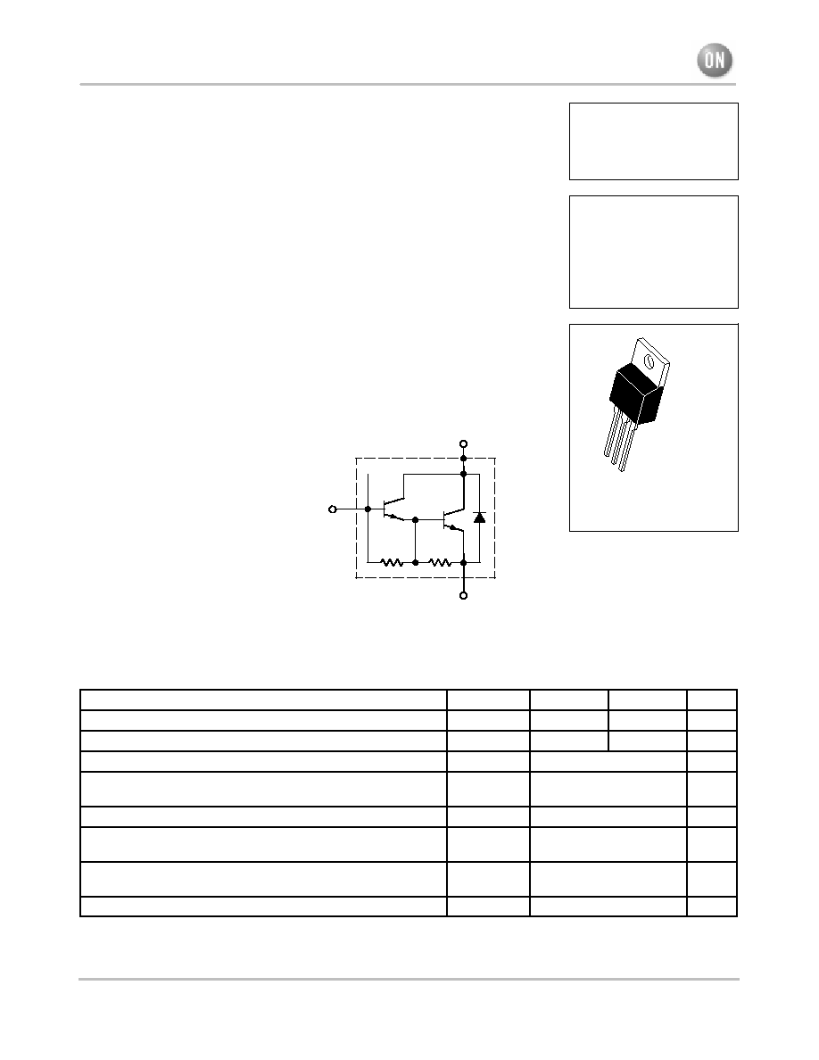
COLLECTOR
EMITTER
[ 8 k
[ 120
Figure 1. Darlington Schematic
BASE
╬╬╬╬╬╬╬╬╬╬╬╬╬╬╬╬╬╬╬╬╬╬╬╬╬╬╬╬╬╬╬╬╬
╬╬╬╬╬╬╬╬╬╬╬╬╬╬╬╬╬╬╬╬╬╬╬╬╬╬╬╬╬╬╬╬╬
MAXIMUM RATINGS (1)
╬╬╬╬╬╬╬╬╬╬╬╬╬╬╬╬╬╬╬
╬╬╬╬╬╬╬╬╬╬╬╬╬╬╬╬╬╬╬
Rating
╬╬╬╬╬
╬╬╬╬╬
Symbol
╬╬╬╬╬
╬╬╬╬╬
2N6667
╬╬╬╬╬
╬╬╬╬╬
2N6668
╬╬╬
╬╬╬
Unit
╬╬╬╬╬╬╬╬╬╬╬╬╬╬╬╬╬╬╬
╬╬╬╬╬╬╬╬╬╬╬╬╬╬╬╬╬╬╬
CollectorşEmitter Voltage
╬╬╬╬╬
╬╬╬╬╬
VCEO
╬╬╬╬╬
╬╬╬╬╬
60
╬╬╬╬╬
╬╬╬╬╬
80
╬╬╬
╬╬╬
Vdc
╬╬╬╬╬╬╬╬╬╬╬╬╬╬╬╬╬╬╬
╬╬╬╬╬╬╬╬╬╬╬╬╬╬╬╬╬╬╬
CollectorşBase Voltage
╬╬╬╬╬
╬╬╬╬╬
VCB
╬╬╬╬╬
╬╬╬╬╬
60
╬╬╬╬╬
╬╬╬╬╬
80
╬╬╬
╬╬╬
Vdc
╬╬╬╬╬╬╬╬╬╬╬╬╬╬╬╬╬╬╬
╬╬╬╬╬╬╬╬╬╬╬╬╬╬╬╬╬╬╬
EmitterşBase Voltage
╬╬╬╬╬
╬╬╬╬╬
VEB
╬╬╬╬╬╬╬╬╬
╬╬╬╬╬╬╬╬╬
5
╬╬╬
╬╬╬
Vdc
╬╬╬╬╬╬╬╬╬╬╬╬╬╬╬╬╬╬╬
╬
╬╬╬╬╬╬╬╬╬╬╬╬╬╬╬╬╬
╬
╬╬╬╬╬╬╬╬╬╬╬╬╬╬╬╬╬╬╬
Collector Current -- Continuous
-- Peak
╬╬╬╬╬
╬
╬╬╬
╬
╬╬╬╬╬
IC
╬╬╬╬╬╬╬╬╬
╬
╬╬╬╬╬╬╬
╬
╬╬╬╬╬╬╬╬╬
10
15
╬╬╬
╬
╬
╬
╬╬╬
Adc
╬╬╬╬╬╬╬╬╬╬╬╬╬╬╬╬╬╬╬
╬╬╬╬╬╬╬╬╬╬╬╬╬╬╬╬╬╬╬
Base Current
╬╬╬╬╬
╬╬╬╬╬
IB
╬╬╬╬╬╬╬╬╬
╬╬╬╬╬╬╬╬╬
250
╬╬╬
╬╬╬
mAdc
╬╬╬╬╬╬╬╬╬╬╬╬╬╬╬╬╬╬╬
╬╬╬╬╬╬╬╬╬╬╬╬╬╬╬╬╬╬╬
Total Device Dissipation @ TC = 25
_
C
Derate above 25
_
C
╬╬╬╬╬
╬╬╬╬╬
PD
╬╬╬╬╬╬╬╬╬
╬╬╬╬╬╬╬╬╬
65
0.52
╬╬╬
╬╬╬
watts
W/
_
C
╬╬╬╬╬╬╬╬╬╬╬╬╬╬╬╬╬╬╬
╬
╬╬╬╬╬╬╬╬╬╬╬╬╬╬╬╬╬
╬
╬╬╬╬╬╬╬╬╬╬╬╬╬╬╬╬╬╬╬
Total Device Dissipation @ TA = 25
_
C
Derate above 25
_
C
╬╬╬╬╬
╬
╬╬╬
╬
╬╬╬╬╬
PD
╬╬╬╬╬╬╬╬╬
╬
╬╬╬╬╬╬╬
╬
╬╬╬╬╬╬╬╬╬
2
0.016
╬╬╬
╬
╬
╬
╬╬╬
Watts
W/
_
C
╬╬╬╬╬╬╬╬╬╬╬╬╬╬╬╬╬╬╬
╬╬╬╬╬╬╬╬╬╬╬╬╬╬╬╬╬╬╬
Operating and Storage Junction Temperature Range
╬╬╬╬╬
╬╬╬╬╬
TJ, Tstg
╬╬╬╬╬╬╬╬╬
╬╬╬╬╬╬╬╬╬
ş65 to +150
╬╬╬
╬╬╬
_
C
(1) Indicates JEDEC Registered Data.
ON Semiconductor
)
ę
Semiconductor Components Industries, LLC, 2002
April, 2002 ş Rev. 4
1
Publication Order Number:
2N6667/D
2N6667
2N6668
PNP SILICON
DARLINGTON
POWER TRANSISTORS
10 AMPERES
60ş80 VOLTS
65 WATTS
CASE 221Aş09
TOş220AB
STYLE 1:
PIN 1. BASE
2. COLLECTOR
3. EMITTER
4. COLLECTOR
1
2
3
4
2N6667 2N6668
http://onsemi.com
2
╬╬╬╬╬╬╬╬╬╬╬╬╬╬╬╬╬╬╬╬╬╬╬╬╬╬╬╬╬╬╬╬╬
╬╬╬╬╬╬╬╬╬╬╬╬╬╬╬╬╬╬╬╬╬╬╬╬╬╬╬╬╬╬╬╬╬
THERMAL CHARACTERISTICS
╬╬╬╬╬╬╬╬╬╬╬╬╬╬╬╬╬╬╬╬╬╬
╬╬╬╬╬╬╬╬╬╬╬╬╬╬╬╬╬╬╬╬╬╬
Characteristic
╬╬╬╬╬
╬╬╬╬╬
Symbol
╬╬╬╬╬╬
╬╬╬╬╬╬
Max
╬╬╬
╬╬╬
Unit
╬╬╬╬╬╬╬╬╬╬╬╬╬╬╬╬╬╬╬╬╬╬
╬╬╬╬╬╬╬╬╬╬╬╬╬╬╬╬╬╬╬╬╬╬
Thermal Resistance, Junction to Case
╬╬╬╬╬
╬╬╬╬╬
R
JC
╬╬╬╬╬╬
╬╬╬╬╬╬
1.92
╬╬╬
╬╬╬
_
C/W
╬╬╬╬╬╬╬╬╬╬╬╬╬╬╬╬╬╬╬╬╬╬
╬╬╬╬╬╬╬╬╬╬╬╬╬╬╬╬╬╬╬╬╬╬
Thermal Resistance, Junction to Ambient
╬╬╬╬╬
╬╬╬╬╬
R
JA
╬╬╬╬╬╬
╬╬╬╬╬╬
62.5
╬╬╬
╬╬╬
_
C/W
╬╬╬╬╬╬╬╬╬╬╬╬╬╬╬╬╬╬╬╬╬╬╬╬╬╬╬╬╬╬╬╬╬
╬╬╬╬╬╬╬╬╬╬╬╬╬╬╬╬╬╬╬╬╬╬╬╬╬╬╬╬╬╬╬╬╬
*ELECTRICAL CHARACTERISTICS
(TC = 25
_
C unless otherwise noted)
╬╬╬╬╬╬╬╬╬╬╬╬╬╬╬╬╬╬╬╬╬╬
╬╬╬╬╬╬╬╬╬╬╬╬╬╬╬╬╬╬╬╬╬╬
Characteristic
╬╬╬╬╬
╬╬╬╬╬
Symbol
╬╬╬
╬╬╬
Min
╬╬╬╬
╬╬╬╬
Max
╬╬╬
╬╬╬
Unit
╬╬╬╬╬╬╬╬╬╬╬╬╬╬╬╬╬╬╬╬╬╬╬╬╬╬╬╬╬╬╬╬╬
╬╬╬╬╬╬╬╬╬╬╬╬╬╬╬╬╬╬╬╬╬╬╬╬╬╬╬╬╬╬╬╬╬
OFF CHARACTERISTICS
╬╬╬╬╬╬╬╬╬╬╬╬╬╬╬╬╬╬╬╬╬╬
╬╬╬╬╬╬╬╬╬╬╬╬╬╬╬╬╬╬╬╬╬╬
CollectorşEmitter Sustaining Voltage (2)
2N6667
(IC = 200 mAdc, IB = 0)
2N6668
╬╬╬╬╬
╬╬╬╬╬
VCEO(sus)
╬╬╬
╬╬╬
60
80
╬╬╬╬
╬╬╬╬
--
--
╬╬╬
╬╬╬
Vdc
╬╬╬╬╬╬╬╬╬╬╬╬╬╬╬╬╬╬╬╬╬╬
╬
╬╬╬╬╬╬╬╬╬╬╬╬╬╬╬╬╬╬╬╬
╬
╬╬╬╬╬╬╬╬╬╬╬╬╬╬╬╬╬╬╬╬╬╬
Collector Cutoff Current (VCE = 60 Vdc, IB = 0)
2N6667
(VCE = 80 Vdc, IB = 0)
2N6668
╬╬╬╬╬
╬
╬╬╬
╬
╬╬╬╬╬
ICEO
╬╬╬
╬
╬
╬
╬╬╬
--
--
╬╬╬╬
╬
╬╬
╬
╬╬╬╬
1
1
╬╬╬
╬
╬
╬
╬╬╬
mAdc
╬╬╬╬╬╬╬╬╬╬╬╬╬╬╬╬╬╬╬╬╬╬
╬
╬╬╬╬╬╬╬╬╬╬╬╬╬╬╬╬╬╬╬╬
╬
╬
╬╬╬╬╬╬╬╬╬╬╬╬╬╬╬╬╬╬╬╬
╬
╬╬╬╬╬╬╬╬╬╬╬╬╬╬╬╬╬╬╬╬╬╬
Collector Cutoff Current
(VCE = 60 Vdc, VEB(off) = 1.5 Vdc)
2N6667
(VCE = 80 Vdc, VEB(off) = 1.5 Vdc)
2N6668
(VCE = 60 Vdc, VEB(off) = 1.5 Vdc, TC = 125
_
C)
2N6667
(VCE = 80 Vdc, VEB(off) = 1.5 Vdc, TC = 125
_
C)
2N6668
╬╬╬╬╬
╬
╬╬╬
╬
╬
╬╬╬
╬
╬╬╬╬╬
ICEX
╬╬╬
╬
╬
╬
╬
╬
╬
╬╬╬
--
--
--
--
╬╬╬╬
╬
╬╬
╬
╬
╬╬
╬
╬╬╬╬
300
300
3
3
╬╬╬
╬
╬
╬
╬
╬
╬
╬╬╬
Á
Adc
mAdc
╬╬╬╬╬╬╬╬╬╬╬╬╬╬╬╬╬╬╬╬╬╬
╬╬╬╬╬╬╬╬╬╬╬╬╬╬╬╬╬╬╬╬╬╬
Emitter Cutoff Current (VBE = 5 Vdc, IC = 0)
╬╬╬╬╬
╬╬╬╬╬
IEBO
╬╬╬
╬╬╬
--
╬╬╬╬
╬╬╬╬
5
╬╬╬
╬╬╬
mAdc
╬╬╬╬╬╬╬╬╬╬╬╬╬╬╬╬╬╬╬╬╬╬╬╬╬╬╬╬╬╬╬╬╬
╬╬╬╬╬╬╬╬╬╬╬╬╬╬╬╬╬╬╬╬╬╬╬╬╬╬╬╬╬╬╬╬╬
ON CHARACTERISTICS (1)
╬╬╬╬╬╬╬╬╬╬╬╬╬╬╬╬╬╬╬╬╬╬
╬
╬╬╬╬╬╬╬╬╬╬╬╬╬╬╬╬╬╬╬╬
╬
╬╬╬╬╬╬╬╬╬╬╬╬╬╬╬╬╬╬╬╬╬╬
DC Current Gain (IC = 5 Adc, VCE = 3 Vdc)
(IC = 10 Adc, VCE = 3 Vdc)
╬╬╬╬╬
╬
╬╬╬
╬
╬╬╬╬╬
hFE
╬╬╬
╬
╬
╬
╬╬╬
1000
100
╬╬╬╬
╬
╬╬
╬
╬╬╬╬
20000
--
╬╬╬
╬
╬
╬
╬╬╬
--
╬╬╬╬╬╬╬╬╬╬╬╬╬╬╬╬╬╬╬╬╬╬
╬╬╬╬╬╬╬╬╬╬╬╬╬╬╬╬╬╬╬╬╬╬
CollectorşEmitter Saturation Voltage (IC = 5 Adc, IB = 0.01 Adc)
(IC = 10 Adc, IB = 0.1 Adc)
╬╬╬╬╬
╬╬╬╬╬
VCE(sat)
╬╬╬
╬╬╬
--
--
╬╬╬╬
╬╬╬╬
2
3
╬╬╬
╬╬╬
Vdc
╬╬╬╬╬╬╬╬╬╬╬╬╬╬╬╬╬╬╬╬╬╬
╬
╬╬╬╬╬╬╬╬╬╬╬╬╬╬╬╬╬╬╬╬
╬
╬╬╬╬╬╬╬╬╬╬╬╬╬╬╬╬╬╬╬╬╬╬
BaseşEmitter Saturation Voltage(IC = 5 Adc, IB = 0.01 Adc)
(IC = 10 Adc, IB = 0.1 Adc)
╬╬╬╬╬
╬
╬╬╬
╬
╬╬╬╬╬
VBE(sat)
╬╬╬
╬
╬
╬
╬╬╬
--
--
╬╬╬╬
╬
╬╬
╬
╬╬╬╬
2.8
4.5
╬╬╬
╬
╬
╬
╬╬╬
Vdc
╬╬╬╬╬╬╬╬╬╬╬╬╬╬╬╬╬╬╬╬╬╬╬╬╬╬╬╬╬╬╬╬╬
╬╬╬╬╬╬╬╬╬╬╬╬╬╬╬╬╬╬╬╬╬╬╬╬╬╬╬╬╬╬╬╬╬
DYNAMIC CHARACTERISTICS
╬╬╬╬╬╬╬╬╬╬╬╬╬╬╬╬╬╬╬╬╬╬
╬╬╬╬╬╬╬╬╬╬╬╬╬╬╬╬╬╬╬╬╬╬
Current Gain -- Bandwidth Product (IC = 1 Adc, VCE = 5 Vdc, ftest = 1 MHz)
╬╬╬╬╬
╬╬╬╬╬
|hfe|
╬╬╬
╬╬╬
20
╬╬╬╬
╬╬╬╬
--
╬╬╬
╬╬╬
--
╬╬╬╬╬╬╬╬╬╬╬╬╬╬╬╬╬╬╬╬╬╬
╬╬╬╬╬╬╬╬╬╬╬╬╬╬╬╬╬╬╬╬╬╬
Output Capacitance (VCB = 10 Vdc, IE = 0, f = 1 MHz)
╬╬╬╬╬
╬╬╬╬╬
Cob
╬╬╬
╬╬╬
--
╬╬╬╬
╬╬╬╬
200
╬╬╬
╬╬╬
pF
╬╬╬╬╬╬╬╬╬╬╬╬╬╬╬╬╬╬╬╬╬╬
╬╬╬╬╬╬╬╬╬╬╬╬╬╬╬╬╬╬╬╬╬╬
SmallşSignal Current Gain (IC = 1 Adc, VCE = 5 Vdc, f = 1 kHz)
╬╬╬╬╬
╬╬╬╬╬
hfe
╬╬╬
╬╬╬
1000
╬╬╬╬
╬╬╬╬
--
╬╬╬
╬╬╬
--
*Indicates JEDEC Registered Data
(2) Pulse Test: Pulse Width
v
300
Á
s, Duty Cycle
v
2%.
Figure 2. Switching Times Test Circuit
0
VCC
- 30 V
SCOPE
TUT
+ 4.0 V
tr, tf v 10 ns
DUTY CYCLE = 1.0%
RC
D1, MUST BE FAST RECOVERY TYPES e.g.,
1N5825 USED ABOVE IB [ 100 mA
MSD6100 USED BELOW IB [ 100 mA
25
Á
s
D1
51
RB & RC VARIED TO OBTAIN DESIRED CURRENT LEVELS
V2
APPROX
+ 8 V
V1
APPROX
- 12 V
[ 8 k
[ 120
FOR td AND tr, D1 IS DISCONNECTED AND V2 = 0
RB
2N6667 2N6668
http://onsemi.com
3
t, TIME
(s)
Á
80
40
20
0
20
40
80
100
120
160
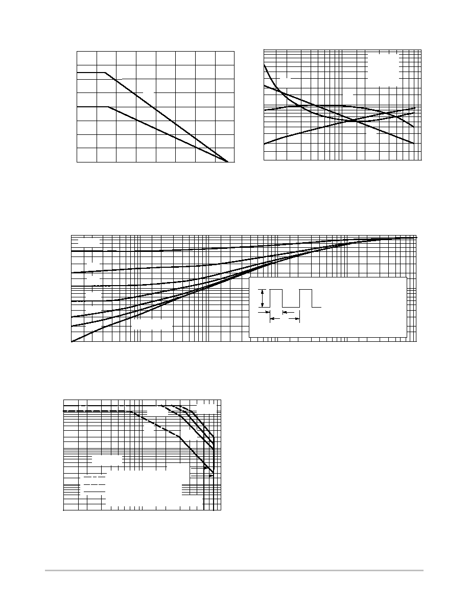
Figure 3. Power Derating
T, TEMPERATURE (
░
C)
P D
, POWER DISSIP
A
TION (W
A
TTS)
60
TA TC
4
2
1
3
0
60
140
TA
TC
0.1
Figure 4. Typical Switching Times
IC, COLLECTOR CURRENT (AMPS)
5
0.7
0.3
0.2
0.2
10
VCC = 30 V
IC/IB = 250
IB1 = IB2
TJ = 25
░
C
tf
1
5
ts
tr
0.1
1
3
0.5
2
.td
0.5
2
7
0.3
0.7
3
7
10
Figure 5. Thermal Response
t, TIME (ms)
1
0.01
0.01
0.5
0.3
0.2
0.1
0.05
0.03
0.02
0.02
r(t) NORMALIZED EFFECTIVE
TRANSIENT
THERMAL
RESIST
ANCE
0.05
0.1
0.2
0.5
1
2
5
10
20
50
100
200
1000
500
Z
JC(t) = r(t) R
JC
R
JC = 1.92
░
C/W MAX
D CURVES APPLY FOR POWER
PULSE TRAIN SHOWN
READ TIME AT t1
TJ(pk) - TC = P(pk) R
JC(t)
P(pk)
t1
t2
DUTY CYCLE, D = t1/t2
D = 0.5
SINGLE PULSE
0.05
0.1
0.02
0.01
0.2
BONDING WIRE LIMIT
THERMAL LIMIT @ TC = 25
░
C
SECOND BREAKDOWN LIMIT
20
1
Figure 6. Maximum Safe Operating Area
2
0.02
10
20
100
TJ = 150
░
C
0.2
5
0.5
I C
, COLLECT
OR CURRENT
(AMPS)
VCE, COLLECTOR-EMITTER VOLTAGE (VOLTS)
10
50
1
0.1
dc
2
70
3
7
2N6667
2N6668
CURVES APPLY BELOW RATED VCEO
1 ms
100
Á
s
5 ms
3
0.03
0.05
0.3
5
30
There are two limitations on the power handling ability of
a transistor: average junction temperature and second
breakdown. Safe operating area curves indicate IC ş VCE
limits of the transistor that must be observed for reliable
operation; i.e., the transistor must not be subjected to greater
dissipation than the curves indicate.
The data of Figure 6 is based on TJ(pk) = 150_C; TC is
variable depending on conditions. Second breakdown pulse
limits are valid for duty cycles to 10% provided TJ(pk)
< 150
_C. TJ(pk) may be calculated from the data in Figure 5.
At high case temperatures, thermal limitations will reduce
the power that can be handled to values less than the
limitations imposed by second breakdown.

2N6667 2N6668
http://onsemi.com
4
10,000
1
Figure 7. Typical SmallşSignal Current Gain
f, FREQUENCY (kHz)
10
2
5
10
20
50
100 200
1000
500
100
5000
h FE
, SMALL-SIGNAL
CURENT
GAIN
20
200
500
2000
1000
50
TC = 25
░
C
VCE = 4 VOLTS
IC = 3 AMPS
300
0.1
Figure 8. Typical Capacitance
VR, REVERSE VOLTAGE (VOLTS)
30
1
2
5
20
100
10
C, CAP
ACIT
ANCE (pF)
200
100
70
50
Cib
Cob
50
0.2
0.5
TJ = 25
░
C
3
7
70
30
300
V CE
, COLLECT
OR-EMITTER VOL
T
AGE (VOL
TS)
0.1
Figure 9. Typical DC Current Gain
IC, COLLECTOR CURRENT (AMPS)
0.2 0.3
0.5 0.7 1
2
10
500
300
h FE
, DC CURRENT
GAIN
TJ = 150
░
C
VCE = 3 V
200
7
20,000
5000
10,000
3000
2000
1000
3
5
Figure 10. Typical Collector Saturation Region
2.6
IB, BASE CURRENT (mA)
0.3
0.5
1
2
3
5
7
30
2.2
1.8
1.4
1
IC = 2 A
TJ = 25
░
C
4 A
6 A
0.6
0.7
20
10
TJ = - 55
░
C
7000
700
TJ = 25
░
C
IC, COLLECTOR CURRENT (AMPS)
VBE(sat) @ IC/IB = 250
V
,
VOL
T
AGE (VOL
TS)
Figure 11. Typical "On" Voltages
VCE(sat) @ IC/IB = 250
TJ = 25
░
C
VBE @ VCE = 3 V
0.1
0.2 0.3
0.5 0.7
1
2
10
7
3
5
3
2
1.5
1
0.5
Figure 12. Typical Temperature Coefficients
+3
+2
0
-1
-2
-3
+5
+4
+1
2.5
0.1
0.2 0.3
0.5 0.7
1
2
10
7
3
5
IC, COLLECTOR CURRENT (AMP)
V,
TEMPERA
TURE COEFFICIENTS (mV/
C)
░
-55
░
C to 25
░
C
25
░
C to 150
░
C
-55
░
C to 25
░
C
25
░
C to 150
░
C
VB for VBE
-4
-5
VC for VCE(sat)
hFE @ VCE + 3.0 V
3
*IC/IB

2N6667 2N6668
http://onsemi.com
5
105
Figure 13. Typical Collector CutşOff Region
VBE, BASE-EMITTER VOLTAGE (VOLTS)
102
101
100
, COLLECT
OR CURRENT
(A)
Á
I C
10-1
VCE = 30 V
TJ = 150
░
C
100
░
C
25
░
C
REVERSE
FORWARD
103
104
+0.2
+0.4
0 -0.2 -0.4 -0.6 -0.8
-1.2 -1.4
-1
+0.6
2N6667 2N6668
http://onsemi.com
6
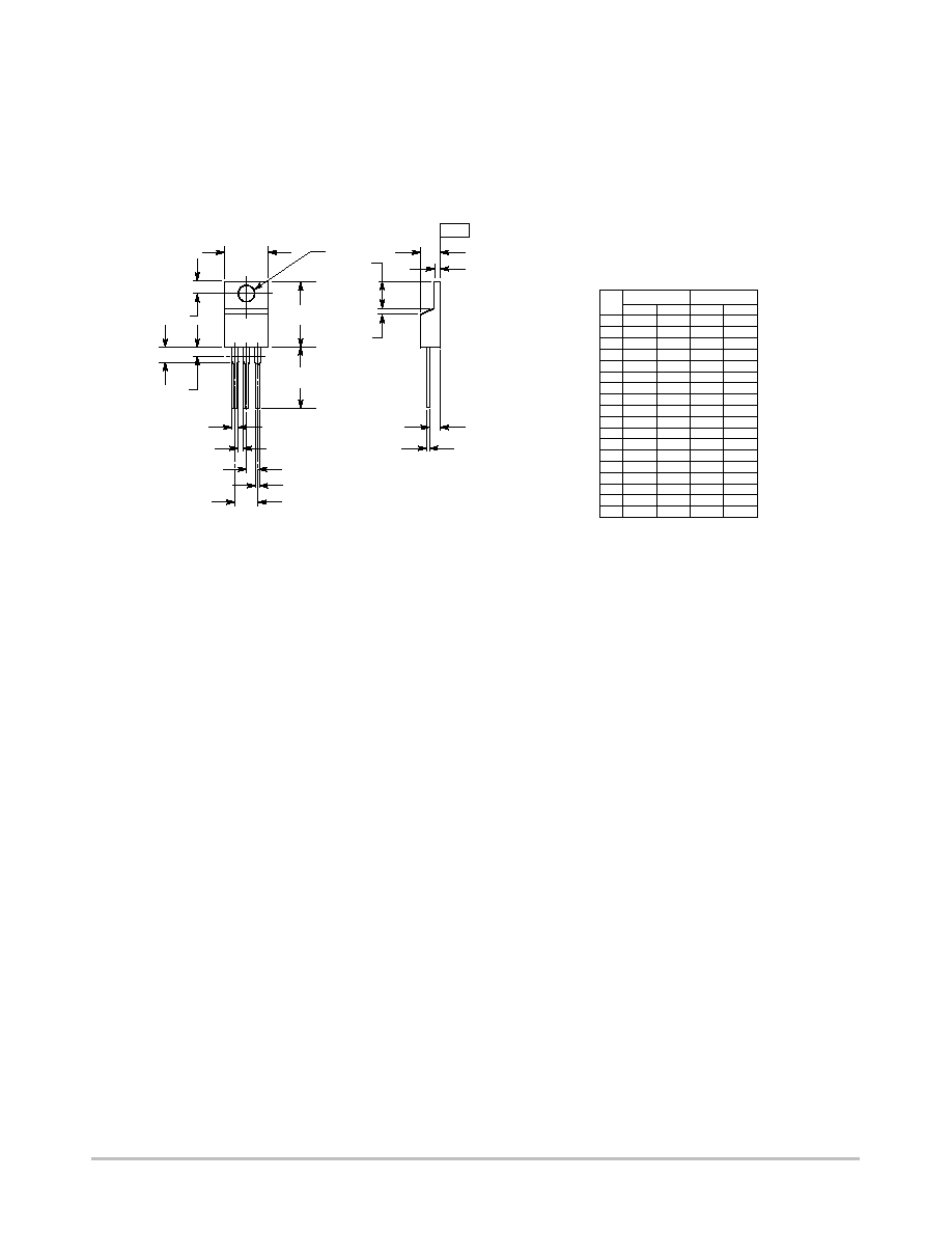
PACKAGE DIMENSIONS
CASE 221Aş09
ISSUE AA
TOş220
NOTES:
1. DIMENSIONING AND TOLERANCING PER ANSI
Y14.5M, 1982.
2. CONTROLLING DIMENSION: INCH.
3. DIMENSION Z DEFINES A ZONE WHERE ALL
BODY AND LEAD IRREGULARITIES ARE
ALLOWED.
DIM
MIN
MAX
MIN
MAX
MILLIMETERS
INCHES
A
0.570
0.620
14.48
15.75
B
0.380
0.405
9.66
10.28
C
0.160
0.190
4.07
4.82
D
0.025
0.035
0.64
0.88
F
0.142
0.147
3.61
3.73
G
0.095
0.105
2.42
2.66
H
0.110
0.155
2.80
3.93
J
0.018
0.025
0.46
0.64
K
0.500
0.562
12.70
14.27
L
0.045
0.060
1.15
1.52
N
0.190
0.210
4.83
5.33
Q
0.100
0.120
2.54
3.04
R
0.080
0.110
2.04
2.79
S
0.045
0.055
1.15
1.39
T
0.235
0.255
5.97
6.47
U
0.000
0.050
0.00
1.27
V
0.045
---
1.15
---
Z
---
0.080
---
2.04
B
Q
H
Z
L
V
G
N
A
K
F
1 2 3
4
D
SEATING
PLANE
şTş
C
S
T
U
R
J
STYLE 1:
PIN 1. BASE
2. COLLECTOR
3. EMITTER
4. COLLECTOR

2N6667 2N6668
http://onsemi.com
7
Notes

2N6667 2N6668
http://onsemi.com
8
ON Semiconductor and are registered trademarks of Semiconductor Components Industries, LLC (SCILLC). SCILLC reserves the right to make
changes without further notice to any products herein. SCILLC makes no warranty, representation or guarantee regarding the suitability of its products for any
particular purpose, nor does SCILLC assume any liability arising out of the application or use of any product or circuit, and specifically disclaims any and all
liability, including without limitation special, consequential or incidental damages. "Typical" parameters which may be provided in SCILLC data sheets and/or
specifications can and do vary in different applications and actual performance may vary over time. All operating parameters, including "Typicals" must be
validated for each customer application by customer's technical experts. SCILLC does not convey any license under its patent rights nor the rights of others.
SCILLC products are not designed, intended, or authorized for use as components in systems intended for surgical implant into the body, or other applications
intended to support or sustain life, or for any other application in which the failure of the SCILLC product could create a situation where personal injury or death
may occur. Should Buyer purchase or use SCILLC products for any such unintended or unauthorized application, Buyer shall indemnify and hold SCILLC
and its officers, employees, subsidiaries, affiliates, and distributors harmless against all claims, costs, damages, and expenses, and reasonable attorney fees
arising out of, directly or indirectly, any claim of personal injury or death associated with such unintended or unauthorized use, even if such claim alleges that
SCILLC was negligent regarding the design or manufacture of the part. SCILLC is an Equal Opportunity/Affirmative Action Employer.
PUBLICATION ORDERING INFORMATION
JAPAN: ON Semiconductor, Japan Customer Focus Center
4ş32ş1 NishişGotanda, Shinagawaşku, Tokyo, Japan 141ş0031
Phone: 81ş3ş5740ş2700
Email: r14525@onsemi.com
ON Semiconductor Website: http://onsemi.com
For additional information, please contact your local
Sales Representative.
2N6667/D
Literature Fulfillment:
Literature Distribution Center for ON Semiconductor
P.O. Box 5163, Denver, Colorado 80217 USA
Phone: 303ş675ş2175 or 800ş344ş3860 Toll Free USA/Canada
Fax: 303ş675ş2176 or 800ş344ş3867 Toll Free USA/Canada
Email: ONlit@hibbertco.com
N. American Technical Support: 800ş282ş9855 Toll Free USA/Canada