
OKI Semiconductor
FEDL9811FULL-04
Issue Date: Sep. 1, 2004
MSM9811
4-Channel Mixing OKI ADPCM Type Voice Synthesis LSI
1/44
GENERAL DESCRIPTION
The MSM9811 is a 4-channel mixing voice synthesis LSI, to which up to 128 Mbits of ROM and/or EPROM
storing voice data can directly be connected externally.
The device is straight 8-bit PCM playback, non-linear 8-bit PCM playback, 4-bit ADPCM playback, and 4-bit
ADPCM2 playback selectable and provides 2-channel stereo output and volume control. The MSM9811 contains
a 14-bit D/A converter and LPF.
The MSM9811 can easily configure a system by connecting voice data storage memory, power amplifier, and
CPU externally.
FEATURES
· Non-linear 8-bit PCM/straight 8-bit PCM/4-bit ADPCM/4-bit ADPCM2
· Serial input or parallel input selectable
· Phrase Control Table function
· 4-channel mixing function
· Master clock frequency
: 4.096 MHz
· Sampling frequency
: 4.0 kHz, 5.3 kHz, 6.4 kHz, 8.0 kHz, 10.6 kHz, 12.8 kHz, 16.0 kHz,
21.2 kHz, 25.6 kHz, 32.0 kHz
· Maximum number of phrases : 256
· Output channel
: L/R 2 channels
· Built-in volume control function (for each output channel)
· Built-in 14-bit D/A converter
· Built-in low-pass filter
: Digital filter
· Package
: 64-pin plastic QFP (QFP64-P-1414-0.80-BK) (MSM9811GA)

FEDL9811FULL-04
OKI Semiconductor
MSM9811
2/44
BLOCK DIAGRAM
D7
/SD
D6
/SI
D5
/S0
S4/UD
D3
/SR3
D2
/SR2
D1
/SR1
D0
/SR0
RC
S CS WR RD
CM
D
SERIAL
NCR/
BU
S
Y
TE
S
T
1
TE
S
T
2
TE
S
T
3
TE
S
T
4
X
T
X
T
8
8
8
16
8-Bit LAT
C
H
23-Bit M
u
ltip
lex
e
r
23-Bit A
ddre
s
s
C
ounter
DAT
A
C
ontrol
l
er
T
i
mi
ng C
o
ntrol
l
er
OSC
CPU
interf
ace
PAN
R
egist
er
14-Bit DAC
14-Bit DAC
ADPC
M
Sy
nthesiz
er
PC
M
Sy
nthesiz
er
16*
9 M
P
Y
RD0
RD7
RA0
RA2
3
R
O
E
RDAO
A
GND
A
V
DD
DGND
DV
DD
R
ES
E
T
LD
AO

FEDL9811FULL-04
OKI Semiconductor
MSM9811
3/44
PIN CONFIGURATION (TOP VIEW)
1
2
3
4
5
6
7
8
9
10
11
12
13
14
15
16
48
47
46
45
44
43
42
41
40
39
38
37
36
35
34
33
64
63
62
61
60
59
58
57
56
55
54
53
52
51
50
49
17
18
19
20
21
22
23
24
25
26
27
28
29
30
31
32
DGND
AGND
TEST4
LDAO
RDAO
AV
DD
DV
DD
RCS
TEST1
TEST2
XT
XT
TEST3
SERIAL
CMD
RD
DV
DD
RA8
RA7
RA6
RA5
RA4
RA3
RA2
RA1
ROE
RD0
RD1
RD2
RD3
RD4
RD5
RA2
3
RA2
2
RA2
1
RA2
0
RA0
RA1
7
RA1
6
RA1
5
RA1
4
RA1
3
RA1
2
RA1
1
RA1
0
RA9
RA1
9
RA1
8
NC
W
R
NCR/
BU
S
Y
C
S
D0
/SR0
D1
/SR1
D2
/SR2
D3
/SR3
D4
/UD
D5
/SO
D6
/SI
D7
/SD
RE
S
E
T
RD7
RD6
DGND
NC: No connection
64-pin Plastic QFP
FEDL9811FULL-04
OKI Semiconductor
MSM9811
4/44
PIN DESCRIPTIONS
Pin Symbol
Type
Description
40-47, 49-64
RA23-RA0
O
Address pins for external memory. These pins become high impedance
when
RCS
pin is "H".
30, 31, 33-38
RD7-RD0
I
Data pin for external memory. Pull-down resistors are internally
connected to these pins. These pull-down resistors become valid when
the
RCS
pin is "H", and become invalid when the
RCS
pin is "L".
39
ROE
O
Output enable pin for external memory. This pin becomes high
impedance when
RCS
pin is "H".
8
RCS
I
When this pin is "L", RA23 to RA0 and
ROE
pins output address data
and output enable signal.
When this pin is "H", RA23 to RA0 and
ROE
pins become high
impedance.
15
CMD
I
Select pin for Command data or Subcommand data for CPU interface.
When this pin is "H", subcommand input is selected.
When this pin is "L", command input is selected. A pull-up resistor is
internally connected to this pin.
16
RD
I
Read pin for CPU interface.
A pull-up resistor is internally connected to this pin.
18
WR
I
Write pin for CPU interface.
A pull-up resistor is internally connected to this pin.
20
CS
I
Chip select pin for CPU interface. When
CS
is "H",
WR
signal is not
entered in this LSI. A pull-up resistor is internally connected to this pin.
14 SERIAL
I
CPU input interface select pin. When SERIAL is "H", serial input
interface is selected.
When it is "L", parallel input interface is selected.
28 D7/SD
I/O
Data bus pin for CPU interface when parallel input interface is selected.
When
WR
is "L", this pin serves as data input pin.
When
RD
is "L", this pin serves as channel status data output pin.
When serial input interface is selected, this pin serves as serial data
input pin.
27 D6/SI
I/O
Data bus pin for CPU interface when parallel input interface is selected.
When
WR
is "L", this pin serves as data input pin.
When
RD
is "L", this pin serves as channel status output pin.
When serial input interface is selected, this pin serves as serial clock
input pin.
26 D5/SO
I/O
Data bus pin for CPU interface when parallel input interface is selected.
When
WR
is "L", this pin serves as data input pin.
When
RD
is "L", this pin serves as channel status output pin.
When serial input interface is selected, this pin serves as channel status
serial output pin.
FEDL9811FULL-04
OKI Semiconductor
MSM9811
5/44
Pin Symbol
Type
Description
25 D4/UD
I/O
Data bus pin for CPU interface when parallel interface is selected.
When
WR
is "L", this pin serves as data input pin.
When
RD
is "L", this pin serves as channel status output pin.
When serial input interface is selected, fix this pin at GND level.
24 D3/SR3
23 D2/SR2
22 D1/SR1
21 D0/SR0
I/O
Data bus pin for CPU interface when parallel input interface is selected.
When
WR
is "L", this pin serves as data input pin.
When
RD
is "L", this pin serves as channel status output pin.
When serial input interface is selected, this pin serves as channel status
output pin.
Channels 4 thru 1 are output to SR3 thru SR0, respectively.
4
LDAO
O
LEFT side D/A output pin.
5
RDAO
O
RIGHT side D/A output pin.
11 XT I
Crystal or ceramic oscillator connection pin.
A feedback resistor of about 1M
is connected between XT and
XT
.
If necessary, enter external clocks into this pin.
12
XT
O
Crystal or ceramic oscillator connection pin.
When external clocks are used, leave this pin open.
29
RESET
I
When this pin is "L" level, the LSI is initialized. At that time, oscillation
stops and D/A outputs go to GND level.
19 NCR/
BUSY
I
Channel status select pin.
When this pin is "H", NCR signal is output. When it is "L",
BUSY
signal is
output.
9 TEST1
10 TEST2
13 TEST3
3 TEST4
I
Pins for LSI testing. Apply "L" level to these pins.
7, 48
DV
DD
--
Digital power supply pin. A bypass capacitor of 0.1
µ
F or more should
be connected between the DGND pin and the DV
DD
pin.
6 AV
DD
--
Analog power supply pin. A bypass capacitor of 0.1
µ
F or more should
be connected between the AGND pin and the AV
DD
pin.
1, 32
DGND
--
Digital GND pin.
2
AGND
--
Analog GND pin.
FEDL9811FULL-04
OKI Semiconductor
MSM9811
6/44
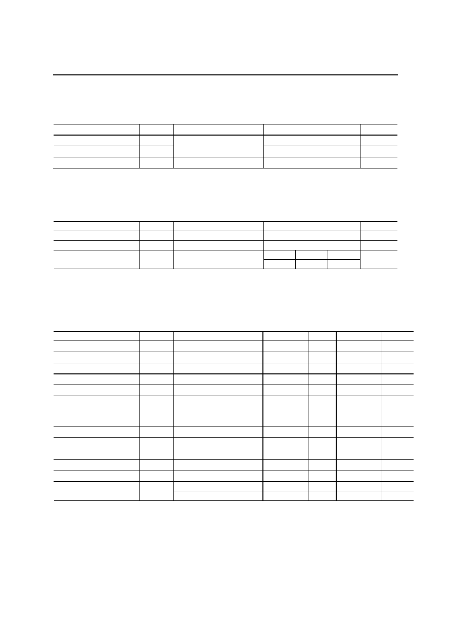
ABSOLUTE MAXIMUM RATINGS
(GND = 0 V)
Parameter Symbol Condition
Rating
Unit
Power Supply Voltage
V
DD
0.3 to +7.0
V
Input Voltage
V
IN
Ta = 25°C
0.3 to V
DD
+ 0.3
V
Storage Temperature
T
STG
--
55 to +150
°C
RECOMMENDED OPERATING CONDITIONS
(GND = 0 V)
Parameter Symbol Condition
Range
Unit
Power Supply Voltage
V
DD
--
4.5 to 5.5
V
Operating Temperature
T
op
--
40 to +85
°C
Min. Typ. Max.
Master Clock Frequency
f
OSC
--
3.5 4.096 4.5
MHz
ELECTRICAL CHARACTERISTICS
DC Characteristics
(DV
DD
= AV
DD
= 4.5 to 5.5 V, DGND = AGND = 0 V, Ta
= 40 to +85°C)
Parameter Symbol Condition Min.
Typ.
Max.
Unit
High-level Input Voltage
V
IH
--
0.84
×
V
DD
-- -- V
Low-level Input Voltage
V
IL
-- --
--
0.16
×
V
DD
V
High-level Output Voltage
V
OH
I
OH
= 1 mA
V
DD
0.4
--
--
V
Low-level Output Voltage
V
OL
I
OL
= 2 mA
--
--
0.4
V
High-level Input Current 1
I
IH1
V
IH
= V
DD
--
--
10
µ
A
High-level Input Current 2
(Note 1)
I
IH2
Applied to pins with internal
pull-down resistor
30 -- 300
µ
A
Low-level Input Current 1
I
IL1
V
IL
= GND
10
--
--
µ
A
Low-level Input Current 2
(Note 2)
I
IL2
Applied to pins with internal
pull-up resistor
300 -- 30
µ
A
Output Leakage Current
I
LO
0
V
OUT
V
DD
10
--
+10
µ
A
Operating Current
I
DD
f
OSC
= 4 MHz, No load
--
6
15
mA
Ta = 40 to +70°C
--
--
15
µ
A
Standby Current
I
DS
Ta = 40 to +85°C
--
--
50
µ
A
Notes 1: Applicable to RD7 to RD0 pins (when RCS = "H").
2:
Applicable
to
CMD, RD, WR, and CS pins.

FEDL9811FULL-04
OKI Semiconductor
MSM9811
7/44
Analog Characteristics
(DV
DD
= AV
DD
= 4.5 to 5.5 V, DGND = AGND = 0 V, Ta = 40 to +85°C)
Parameter Symbol
Condition Min.
Typ.
Max. Unit
LDAO,RDAO Load Resistance
(During OP amplifier output)
R
OUTA
--
50
--
-- k
LDAO,RDAO
Output
Impedance
(When OP amplifier is not used)
R
OUTD
--
--
3
-- k
LDAO,RDAO Output Level
--
No load
--
0.7 to 0.94 V
DD
-- V
AC Characteristics
(V
DD
= 4.5 to 5.5 V, GND = 0 V, Ta = 40 to +85°C, C
L
= 5 pF)
Parameter Symbol
Min.
Typ.
Max.
Unit
Master Clock Duty Cycle
f
duty
40 50 60 %
RESET
Input Pulse Width
t
W(
RST
)
1 -- --
µ
s
RESET
Delay Time From Raising of Power Supply
t
D(
RST
)
0 -- --
µ
s
Set up and Hold Time of
CS
for
RD
t
CR
30 -- -- ns
RD
Pulse Width
t
RR
200 -- -- ns
Output Data Valid Time after Fall of
RD
t
DRE
-- -- 100 ns
Data Float Time after Rise of
RD
t
DRF
-- 10 50 ns
Setup and Hold Time of
CMD
for
WR
t
DW
50 -- -- ns
Setup and Hold Time of
CS
for
WR
t
CW
30 -- -- ns
WR
Pulse Width
t
WW
200 -- -- ns
Data Setup Time before Rise of
WR
t
DWS
100 -- -- ns
Data Hold Time after Rise of
WR
t
DWH
30 -- -- ns
WR
-
WR
Pulse Interval
t
WWS
160 -- -- ns
CS
-
CS
Pulse Interval
t
CC
100 -- -- ns
Serial Data Setup Time
t
SDS
30 -- -- ns
Serial Data Hold Time
t
SSD
30 -- -- ns
Serial Clock Pulse Width
t
W(SCK)
200 -- -- ns
Output Data Valid Time after Rise of Serial Clock
t
SDD
-- -- 200 ns
Setup Time of
WR
for Serial Data
t
SWDS
200 -- -- ns
Setup Time of Serial Clock Fall for
WR
Rise
t
SIWS
300 -- -- ns
Setup Time of
RD
for Serial Clock Rise
t
SRIS
300 -- -- ns
FEDL9811FULL-04
OKI Semiconductor
MSM9811
8/44
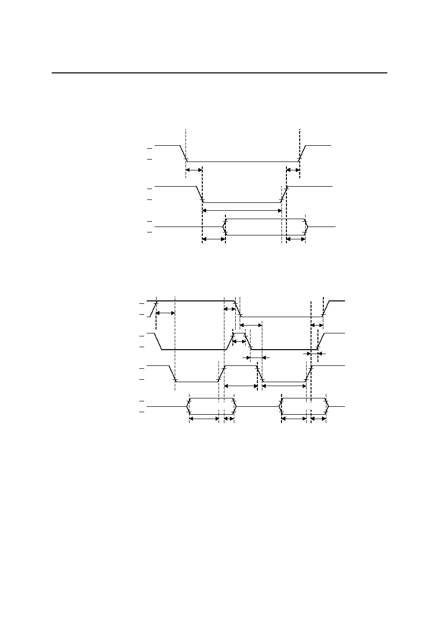
TIMING DIAGRAMS (PARALLEL INPUT)
Data Read Timing
RD
(I)
D7 - D0(O)
t
RR
t
DRE
t
DRF
Data out Valid
CS
(I)
t
CR
t
CR
VIH
VIL
VIH
VIL
VOH
VOL
Data Write Timing (Sub-command, Command Input)
CMD
(I)
CS
(I)
t
WSS
t
DWS
WR
(I)
D7 - D0(I)
t
DWH
t
WW
t
CW
t
DW
t
DW
t
CW
t
DW
t
DW
t
CC
t
DWS
t
DWH
VIH
VIL
VIH
VIL
VIH
VIL
VIH
VIL
Data Stable
Data Stable

FEDL9811FULL-04
OKI Semiconductor
MSM9811
9/44
TIMING DIAGRAMS (SERIAL INPUT)
Data Write Timing (Sub-command, Command Input)
CMD
(I)
CS
(I)
WR
(I)
SD(I)
SI(I)
t
CW
t
DW
t
CC
t
DW
t
CW
t
DW
t
DW
t
WSS
t
SWDS
t
SIWS
t
SIWS
WR
(I)
SD(I)
SI(I)
t
SSD
t
SDS
t
W(SCK)
t
SWDS
t
W(SCK)
t
SSD
t
SDS
t
W(SCK)
t
W(SCK)
VIH
VIL
VIH
VIL
VIH
VIL
VIH
VIL
VIH
VIL
VIH
VIL

FEDL9811FULL-04
OKI Semiconductor
MSM9811
10/44
Data Read Timing
CS
(I)
RD
(I)
SO(O)
SI(I)
t
CR
t
CR
D7 D6 D5 D4 D3 D2 D1
D0
RD
(I)
SO(O)
SI(I)
t
SRIS
VIH
VIL
VIH
VIL
VOH
VOL
VIH
VIL
VIH
VIL
t
SDD
t
SDD

FEDL9811FULL-04
OKI Semiconductor
MSM9811
11/44
TIMING DIAGRAM (COMMON TO PARALLEL AND SERIAL I/O)
Power-on Timing · Power-down Timing
V
DD
RESET
(I)
t
D(
RST
)
t
W(
RST
)
XT
XT
Reset
processing
Waiting for command
Oscillation
stabilization
Oscillating
4.5V
VIH
VIL
Standby
RESET
(I)
t
W(
RST
)
LDAO (O)
RDAO
(O)
XT
XT
Standby
Waiting for command
Waiting for command
1/2V
DD
GND
Oscillating
Oscillation
stabilization
time
GND
1/2V
DD
1/2V
DD
1/2V
DD
Oscillating
FEDL9811FULL-04
OKI Semiconductor
MSM9811
12/44
Continuous Playback Timing When Phrase Control Table is not Used
LD
AO
/RD
A
O
S
u
b
-
co
mm
an
d/
Co
m
m
an
d
N
CRn
BU
S
Y
n
FA
D
R
1
ST
A
R
T
FA
D
R
2
ST
A
R
T
F
A
D
R
1
pl
ay
ba
ck
FA
DR
2
pl
ay
ba
ck
FEDL9811FULL-04
OKI Semiconductor
MSM9811
13/44
Continuous Playback Timing When Phrase Control Table is Used
(
Note)
Do not enter th
e ST
ART
command a
nd MU
ON command
durin
g pl
aybac
k (
BUSY
=
"L")
when th
e phra
s
e control tab
l
e
is used. Otherwise,
the LSI may malfuncti
on. Enter t
he ST
ART
command
and
MUON comma
nd after
BUSY
= "H".
LDA
O
/
R
D
A
O
Su
b
-
c
o
mm
a
n
d
/
Co
m
m
a
n
d
N
CRn
BU
S
Y
n
Not
e
)
F
A
DR1
S
T
A
R
T
FA
D
R
2
STA
R
T
FA
D
R
2
pl
ay
b
a
c
k
F
A
DR1
p
l
a
y
b
a
ck

FEDL9811FULL-04
OKI Semiconductor
MSM9811
14/44
LOOP Playback Timing (Phrase Control Table is Used/not Used)
L
D
A
O
/
RDA
O
Su
b-
c
o
mma
nd
/
C
o
mma
nd
NCRn
BU
S
Y
n
FAD
R
1
STAR
T
LOOP relea
s
e
d
LO
OP
s
e
t
FADR1 play
ba
ck
LOO
P
v
a
l
i
d
FADR1 pl
ay
ba
c
k
LOOP valid
FA
D
R
1 p
l
ay
ba
c
k

FEDL9811FULL-04
OKI Semiconductor
MSM9811
15/44
MUON Command Input Timing When Phrase Control Table is not Used
DAOL/ DAOR
Sub-
c
o
mmand
/
Com
m
a
n
d
N
CRn
BU
S
Y
n
FADR1
ST
AR
T
FADR2
ST
AR
T
M
U
O
N
FADR2 pla
y
b
a
ck
FADR1 pl
ay
b
a
c
k
Sile
n
c
e
(
4
t
o
10
20
m
s
)
MUO
N
c
o
m
m
and

FEDL9811FULL-04
OKI Semiconductor
MSM9811
16/44
MUON Command Input Timing When Phrase Control Table is Used
DAO
L
/DAO
R
S
u
b
-
c
o
mma
nd
/
Com
m
an
d
NC
Rn
BU
S
Y
n
FA
D
R
1
No
te
)
No
te
)
ST
AR
T
FADR
2
ST
AR
T
M
U
O
N
FADR
2
pl
a
y
ba
c
k
FADR1 pl
ay
ba
ck
Si
le
n
c
e (
4
to
10
20
m
s
)
M
U
O
N
co
mman
d
(N
ote)
Do
n
o
t
ent
e
r t
h
e ST
AR
T c
o
mman
d
a
nd
M
U
O
N
c
o
mm
and
d
u
ri
ng
pl
aybac
k
(
BUSY
= "L") whe
n
the
phrase c
ont
rol table is
used.
Oth
e
rwise, th
e
LSI
may malfun
ctio
n.
En
te
r the START
command a
n
d
MUON c
o
mmand a
f
ter
BU
S
Y
=
"H".

FEDL9811FULL-04
OKI Semiconductor
MSM9811
17/44
FUNCTIONAL DESCRIPTION
Microcontroller Interface
The microcontroller interface includes two interface circuits, parallel interface and serial interface.
The statuses of each pin both in parallel interface mode and in serial interface mode are shown below.
SERIAL = "L
"
SERIAL = "H"
Parallel I/O interface
Serial I/O interface
D7 (I/O)
SD (I)
Serial data input pin
D6 (I/O)
SI (I)
Serial clock input pin
D5 (I/O)
SO (O)
Serial data output pin
D4 (I/O)
UD (I)
Fix this pin at GND level
D3 (I/O)
SR3 (O)
D2 (I/O)
SR2 (O)
D1 (I/O)
SR1 (O)
D0 (I/O)
Data I/O pins
SR0 (O)
Channel status signal output pin

FEDL9811FULL-04
OKI Semiconductor
MSM9811
18/44
Command List
Commands
Each command consists of a command and a sub-command.
Data is input when the
CMD pin is "H". A command is input when the CMD pin is "L".
D7 to D0
NCRn
Comman
d name
CMD
pin
7 6 5
4
3
2
1
0
Description
H 0 0 0
0
CH4
to
CH1
Sets the bit of a voice
synthesis start channel to "1".
Valid
only at
"H"
START
L
0 0 0
0
0
X
X
X Starts
playback.
H 0 0 0
0
CH4
to
CH1
Sets the bit of a voice
synthesis end channel to "1".
None STOP
L
0 0 0
0
1
X
X
X Ends
playback.
H 0 0 0
0
CH4
to
CH1
Sets the bit of a LOOP channel
to "1".
None LOOP
L
0 0 0
1
0
X
X
X Starts
LOOP.
H 0 0 0
O
4
O
3
O
2
O
1
O0
Selects an option.
None OPT
L
0 0 0
1
1
X
X
X
H
M7 to M0
Selects a silence time at M
×
4
ms. (Condition: 1
M
255)
Valid
only at
"H"
MUON
L
0
0
1
0
0
0
C1 to C0
Selects a channel that outputs
a silence and plays a silence.
H
FA7 to FA0
Selects a phrase to be played.
None FADR
L
0
0
1
0
1
0
C1 to C0
Selects a channel that sets up
a phrase.
H
SA23 to SA16
H
SA15 to SA8
H
SA7 to SA0
Selects a ROM address at
which voice synthesis starts.
H
ST23 to ST16
H
ST15 to ST8
H ST7
to
ST0
Selects a ROM address at
which voice synthesis ends.
H
S3 to S0
P1 to
P0
0
0
Selects a sampling frequency
using S3 to S0.
Selects a voice synthesis
method using P1 to P0.
None DADR
L
0
0
1
1
0
0
C1 to C0
Sets the condition to a channel
selected by C1 to C0.
H
X
X
X
X
V3 to V0
Sets a playback volume
between V3 and V0
×
2 dB.
None CVOL
L
0
0
1
1
1
0
C1 to C0
Selects a channel to which a
playback volume is set.
H
L3 to L0
R3 to R0
Selects a left side voice
volume using L3 to L0 and
selects a right side voice
volume using R3 to R0. The
volume of output is 2 dB
×
(L
or R).
None PAN
L
0
1
0
0
0
0
C1 to C0
Selects a channel for setting
PAN using C1 to C0.
X: Don't Care

FEDL9811FULL-04
OKI Semiconductor
MSM9811
19/44
Sampling Frequency List
S3 to S0
Sampling Frequency
0 4.0
kHz
1 8.0
kHz
2 16.0
kHz
3 32.0
kHz
4 Undefined
5 6.4
kHz
6 12.8
kHz
7 25.6
kHz
8 Undefined
9 5.3
kHz
10 10.6
kHz
11 21.2
kHz
12 Undefined
13 Undefined
14 Undefined
15 Undefined
Voice Synthesis Algorithm List
P1 to P0
Voice synthesis algorithm
0
OKI 4-bit ADPCM
1
OKI 4-bit ADPCM2
2
8-bit Straight PCM
3
OKI 8-bit Nonlinear PCM

FEDL9811FULL-04
OKI Semiconductor
MSM9811
20/44
PAN and CVOL List
L3 to L0
R3 to R0
V3 to V0
Volume
L3 to L0
R3 to R0
V3 to V0
Volume
0
0 dB
8
16 dB
1
2 dB
9
18 dB
2
4 dB
10
20 dB
3
6 dB
11
22 dB
4
8 dB
12
24 dB
5
10 dB
13
26 dB
6
12 dB
14
28 dB
7
14 dB
15
30 dB
OPT Command List
Default O4 O3 O2 O1 O0
Description
* 0
0 x
x
x
Sets the volumes of all channels to V
DD
(p-p).
0
1
x
x
x
Sets the volumes of all channels to 1/2 V
DD
(p-p).
1
0
x
x
x
Sets the volumes of all channels to 1/4 V
DD
(p-p).
1
1
x
x
x
Sets the volumes of all channels to 1/8 V
DD
(p-p).
*
x
x 0 0 x
Secondary digital filtering is performed.
x
x 0 1 x
Primary digital filtering is performed.
x
x 1 x
x
An on-chip digital filter is not used.
*
x
x
x
x
0
Data is output directly from a D/A converter. (Output Z
3 k
)
x
x
x
x
1
Data is output via a voltage follower. (Output Z
500
)
(Note) x indicates that data is independent of a function described.

FEDL9811FULL-04
OKI Semiconductor
MSM9811
21/44
LPF Frequency Characteristics
This LSI contains a LPF in which a digital filter technology is used. The frequency characteristics when a
secondary filter is used at fs = 8 kHz is shown below. The cutoff frequency is directly proportional to the sampling
frequency fs.
LPF Output Frequency Characteristics (fs = 8 kHz)
-100
-90
-80
-70
-60
-50
-40
-30
-20
-10
0
100
1000
10000
100000
[Hz]
[dB]

FEDL9811FULL-04
OKI Semiconductor
MSM9811
22/44
Power Down Function
To enter the power down mode, set the
RESET pin to "L".
When an external clock is supplied to the XT pin, fix the
XT pin at "L".
If an external clock is supplied via the XT pin during the power down mode, the I
DS
specification is not satisfied
because current flows between the XT pin and the
XT pin.
The circuit of XT and
XT pins is shown below.
Channel Status
The channel status includes NCRn and
BUSYn. These two channel statuses can be switched by setting the
NCR/
BUSY pin.
Corresponding
channel
NCR/
BUSY
= "H"
NCR/
BUSY
= "L"
CH1 NCR1
BUSY
1
CH2 NCR2
BUSY
2
CH3 NCR3
BUSY
3
CH4 NCR4
BUSY
4
The n-channel NCR signal is NCRn and the n-channel
BUSY signal is BUSYn.
When NCRn is "H", the START command and MUON command can be input for the next message of "n" channel
to be played.
When the phrase control table is used and
BUSYn is "L", do not enter the START command and MUON command
even if NCRn is "H".
Otherwise, the LSI may malfunction.
When
BUSYn is "H", the "n" channel does not output a voice.
When
BUSYn is "L", the "n" channel outputs a voice.
Approx. 500 k
RESET
"L"
Internal master clock
XT
"L"
XT
Power down mode

FEDL9811FULL-04
OKI Semiconductor
MSM9811
23/44
Parallel I/O (SERIAL = "L")
The outputs of channel statuses in parallel I/O mode are shown below.
Pin name
NCR/
BUSY
= "H"
NCR/
BUSY
= "L"
D3 NCR4
BUSY
4
D2 NCR3
BUSY
3
D1 NCR2
BUSY
2
D0 NCR1
BUSY
1
Serial I/O (SERIAL = "H")
The outputs when channel statuses are serially read during serial I/O mode are shown below.
Signal name
NCR/
BUSY
= "H"
NCR/
BUSY
= "L"
SO3 NCR4
BUSY
4
SO2 NCR3
BUSY
3
SO1 NCR2
BUSY
2
SO0 NCR1
BUSY
1
The outputs when channel statuses are output via SR3 to SR0 during serial I/O mode are shown below.
Pin name
NCR/
BUSY
= "H"
NCR/
BUSY
= "L"
SR3 NCR4
BUSY
4
SR2 NCR3
BUSY
3
SR1 NCR2
BUSY
2
SR0 NCR1
BUSY
1

FEDL9811FULL-04
OKI Semiconductor
MSM9811
24/44
Voice Synthesis Algorithms
The MSM9811 contains 4-bit ADPCM algorithm, 4-bit ADPCM2 algorithm, 8-bit straight PCM algorithm, and
8-bit non-linear PCM algorithm. One of these algorithms can be selected depending on the kind of voices to be
played. The features of these algorithms are described below.
Voice synthesis algorithm
Applicable waveform
Feature
Oki 4-bit ADPCM
Normal voice waveforms
Oki-original 4-bit ADPCM
Oki 4-bit ADPCM2
Normal voice waveforms
An improved version of Oki-original 4-bit ADPCM.
This algorithm has improved its waveform
traceability.
Oki 8-bit Nonlinear PCM
Sound effects including
high frequency components
This algorithm plays back the center of waveform
as a 10-bit sound.
8-bit PCM
Sound effects including
high frequency components
Normal 8-bit PCM algorithm
Memory Configuration and Voice Data Creation Method
The ROM data consists of a voice management area, a voice data area, and a phrase control table area.
The voice management area controls the voice data start address, voice data end address, and use of the phrase
control table.
256 phrases of voice management data are stored in this area.
The voice data area stores actual waveform data.
The phrase control table area stores data for effectively using voice data. See "Phrase Control Table Function" for
details.
The ROM data is created by using a dedicated tool.
Voice management area
(16 Kbit fixed)
Voice data area
Phrase control table area
This area is used to create
ROM data.
0x000000
0x0007FF
0x000800
max: 0x7ffffff
max: 0x7ffffff
ROM address

FEDL9811FULL-04
OKI Semiconductor
MSM9811
25/44
Playback Time and Memory Capacity
The playback time is determined by external memory capacity, sampling frequency, and voice synthesis algorithm.
The relationship is described below.
(The bit length is 4 bits for ADPCM and ADPCM2 and 8 bits for PCM.)
When the sampling frequency is 16 kHz and the voice synthesis algorithm is 4-bit ADPCM and an 8-Mbit ROM is
used, the playback time is calculated as shown below.
In the above equation, the playback time when the phrase control table function is not used is shown.
1.024
×
(Memory capacity 16) (Kbits)
Sampling frequency (kHz)
×
bit length
Playback time =
(Seconds)
1.024
×
(8192 16) (Kbits)
16 (kHz )
×
4 (bit)
Playback time =
131 (Seconds)

FEDL9811FULL-04
OKI Semiconductor
MSM9811
26/44
Mixing Function
It is possible to mix 4 channels at a time. Moreover, the LSI is capable of starting or stopping voices of each
channel separately.
· Note on waveform clamping during mixing
Increasing the number of channels to be mixed may cause clamping.
To prevent clamping, reduce the volumes of all channels using the OPT command.
(Note)
Mixing using a different sampling frequency cannot be done.
Continuous Playback Function
The continuous playback function is used to continuously play back the next phrase after playing back a phrase.
The next phrase to be played can be previously selected while a phrase is being played back.
See "Continuous Playback Flowchart" for details.
The continuous playback function is also available in the case of the phase control table.
(Note)
The following changes of voice synthesis algorithms are not permitted for continuous playback function. These
changes may generate noises.
·
ADPCM
ADPCM2
·
ADPCM2
ADPCM
FEDL9811FULL-04
OKI Semiconductor
MSM9811
27/44
Phrase Control Table Function
The phrase control table function is used to continuously play back multiple phrases and to set up a volume.
It is possible to perform the following functions using the phrase control table function.
·
CVOL setting
·
Continuous playback (The number of continuous playbacks can be specified limitlessly, but depends on
memory capacity.)
·
Silence insertion function (4 mSec to 124 mSec)
The memory capacity of voice ROM is effectively used by using the phrase control table function.
Examples of ROM data when the phrase control table function is used are shown below.
Example 1) Phrases when the phrase control table function is used
Phrase 1
Phrase 2
Phrase 3
Phrase 4
It
fine
It
is
It
is
It
is
Phrase 5
rainy
tomorrow
tomorrow
is
It
Silence
is
tomorrow
It
rainy
fine
today
today
fine
rainy
today
is
Example 2) ROM data when the example 1 is converted into ROM
Address
management area
Phrase control area
It
fine
rainy
is
today
tomorrow
(Note)
In the phrase control table, each message of the playing phrase is provided with a CVOL value. Note that a CVOL
value is overwritten over each message.
FEDL9811FULL-04
OKI Semiconductor
MSM9811
28/44
Volume Function
·
A volume can be adjusted at the stages of OPT, CVOL and PAN as shown below.
·
A volume is set to all channels at the stage of OPT.
·
A volume is set to each channel at the stage of CVOL.
·
A volume is set to "L" and "R" of each channel at the stage of PAN.
OPT
PAN[L]
CH1
CVOL
CH2
CVOL
CH3
CVOL
CH4
CVOL
PAN[R]
PAN[L]
PAN[R]
PAN[L]
PAN[R]
PAN[L]
PAN[R]
Left-side
Mixing
Block
Left-side
Output
Right-
side
Mixing
Block
Right-
side
Output
ADPCM
Block
The output level attenuations when the CVOL, OPT and PAN commands are executed are shown below.
<Left-side output volume calculation>
Left-side output volume = (V + L)
× 2 + (O4 × 2 + O3) × 6 [dB]
V:
Setting a volume (0 to 15) with the CVOL command
L:
Setting a left-side volume (0 to 15) with the PAN command
O4, O3: Setting a volume (0 or 1) with the OPT command
<Right-side output volume calculation>
Right-side output volume = (V + L) x 2 + (O4
× 2 + O3) × 6 [dB]
V:
Setting a volume (0 to 15) with the CVOL command
L:
Setting a right-side volume (0 to 15) with the PAN command
O4, O3: Setting a volume (0 or 1) with the OPT command

FEDL9811FULL-04
OKI Semiconductor
MSM9811
29/44
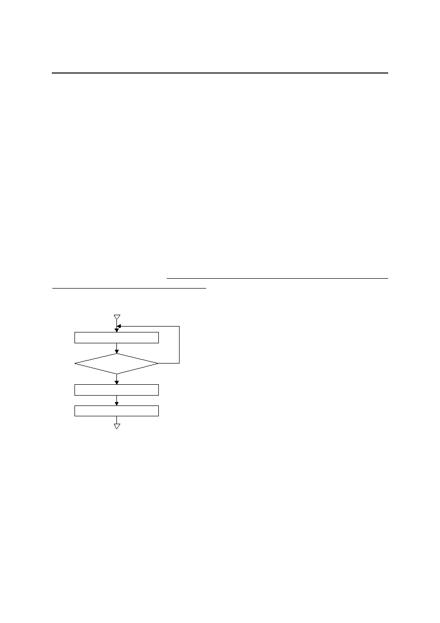
START Command
The START command starts voice synthesis of the channel corresponding to the data stored in the TMP register.
Table 1 shows the correspondence between data input (D7-D0) and channels. In the case of serial input, all 8 bits of
D7 to D0 should be input serially from MSB.
Table 1 Correspondence between D7-D0 and Channels
Data
bus
D7 D6 D5 D4 D3 D2 D1 D0
Corresponding channel
0
0
0
0
CH4
CH3
CH2
CH1
When the START command is input, data stored in the TMP register is set at the start register, and voice synthesis
processing starts. For example, when all "1's" are written from the data bus to the TMP register and the START
command is input, all channels start voice synthesis simultaneously.
Input the START command when the status signal (NCR or
BUSY) of the channel to be started is at "H". When
NCR is "L", input is disabled. When the phrase control table is used, input the START command while
BUSY is
"H". Otherwise, the LSI may malfunction.
Figure 4 shows the flowchart when the START command is input.
Subcommand input
RD
pulse input
NCRn="H"
START command input
No
Yes
NCRn corresponding to each channel is output to D7-D0
Check that D7-D0 corresponding to the channel
to start voice synthesis is "H".
(
BUSY
n is "H" when the phrase control table is used.)
After setting "L" to D7-D0 corresponding to the channel to start
voice synthesis from the data bus, input the
WR
pulse. (Set
CMD
to "H".)
Figure 4 START Command Input Flow
STOP Command
The STOP command stops voice synthesis processing of the channel corresponding to data stored in the TMP
register. Table 2 shows the correspondence between data input (D7-D0) and channels.
Table 2 Correspondence between D7-D0 and channels
Data
bus
D7 D6 D5 D4 D3 D2 D1 D0
Corresponding
channel
0 0 0 0
CH4
CH3
CH2
CH1
When the STOP command is input, the LSI stops processing of voice synthesis of the corresponding channel at the
rise of the
WR pulse. When voice synthesis stops, the PCM value of that channel is cleared to 1/2 V
DD
, and the
NCR and
BUSY channel status signals become "H".
When "H" has been set at the START register, the START register is cleared to "L".

FEDL9811FULL-04
OKI Semiconductor
MSM9811
30/44
LOOP Command
The LOOP command repeats a playback of voice synthesis of the channel corresponding to data stored in the TMP
registers. Table 3 shows the correspondence between data input (D7-D0) and channels.
Table 3 Correspondence between D7-D0 and Channels
Data
bus
D7 D6 D5 D4 D3 D2 D1 D0
Corresponding channel
0
0
0
0
CH4
CH3
CH2
CH1
When the LOOP command is input, the LSI writes data of the TMP register to the LOOP register at rise of
WR
pulse, and repeats a playback of the channel where "H" is set. Once "H" is set at the LOOP register, playback
continues until "L" is set from the outside. If the phrase control table function has been used for a phrase address,
the edited voice is repeatedly played back.
To end a repeating playback, set the register of the channel to end the repeat to "L" using the LOOP command
again. When the register is set to "L", repeating ends with the phrase next to the current playback phrase. If the
START register has been set to continue the playback of another phrase, another phrase is played back
continuously after repeating ends.
Figure 5 shows an example.
Channel 1
LOOP start
Phrase 1
Phrase 1
Phrase 1
Phrase 2
LOOP end
Phrase 1
start
Phrase 1
Phrase 2
start
Figure 5 LOOP Command Execution Example

FEDL9811FULL-04
OKI Semiconductor
MSM9811
31/44
OPT Command
The OPT command changes the setting inside the LSI according to data stored in the TMP register. Table 4 shows
the correspondence between data input (D7 to D0) and options.
Table 4 OPT Command List
Default O4 O3 O2 O1 O0
Description
* 0
0 x
x
x
Sets the volumes of all channels to V
DD
(p-p).
0
1
x
x
x
Sets the volumes of all channels to 1/2 V
DD
(p-p).
1
0
x
x
x
Sets the volumes of all channels to 1/4 V
DD
(p-p).
1
1
x
x
x
Sets the volumes of all channels to 1/8 V
DD
(p-p).
*
x
x 0 0 x
Secondary digital filtering is performed.
x
x 0 1 x
Primary digital filtering is performed.
x
x 1 x
x
An on-chip digital filter is not used.
*
x
x
x
x
0
Data is output directly from a D/A converter. (Output Z
3 k
)
x
x
x
x
1
Data is output via a voltage follower. (Output Z
500
)
(Note) x indicates that data is independent of a function described.
When the OPT command is input, the LSI changes the option at the rising edge of the
WR pulse. When power is
turned on, or when the
RESET pulse is input, the registers corresponding to D4-D0 have been set to "L".
If the option is changed when voice synthesis is in execution, voice quality may change. Oki recommends to set the
option after power is turned on or after
RESET is input.
1)
Volume Option
Volume can be set by the CVOL command and PAN command, but a waveform may be clamped when channel
synthesis is executed.
If the CVOL command and PAN command are used to prevent a waveform from being clamped, the number of
steps used for actual volume decreases, and effective voice synthesis may not be performed.
If it is known that a waveform will be clamped, this option can set the volume of all channels to low, so that the
number of steps of the volume can be utilized to the maximum level.
2)
Digital Filter Processing
This LSI has a built-in oversampling circuit for digital filter processing. This oversampling system evenly
generates four times more points of sampling frequencies.
When power is turned on or if the
RESET pulse is input, those pulses have been set to pass through the
oversampling circuit. If digital filter processing is unnecessary, change this setting by the OPT command.
FEDL9811FULL-04
OKI Semiconductor
MSM9811
32/44
3)
Analog Output
When power is turned on, it has been set that the output of the D/A converter is output via the voltage follower. To
change this setting, use the OPT command.
The output impedance of analog signals being output via the voltage follower is about 500
.
The output impedance of analog signals directly output from the D/A converter is about 3 k
.
MUON Command
The MUON command inserts silence into the specified channel at the rise of the
WR pulse. The length of silence is
according to the size of data stored in the TMP register.
The length of silence data is input in advance, before executing the MUON command. Silence length can be set for
255 steps, 4 ms to 1020 ms, in 4 ms intervals. Silence time can be set as follows.
t
mu
= (2
7
× (D7) + 2
6
× (D6) + 2
5
× (D5) + 2
4
× (D4) + 2
3
× (D3) + 2
2
× (D2) + 2
1
× (D1) + 2
0
× (D0)) × 4.096 ms
The operation of the MUON command is similar to the START command to start voice synthesis. When the
MUON command is input, "H" is set to the START register, and NCR and
BUSY signals becomes "L".
If the MUON command is input when voice synthesis is in execution, silence time is inserted after voice synthesis
ends.
Input the MUON command when the status signal (NCR or
BUSY) of the channel to start voice synthesis is at "H".
When NCR is "L", input is disabled. When the phrase control table is used, input the MUON command while
BUSY is "H". Otherwise, the LSI may malfunction.
Figure 6 shows a flow chart example when the MUON command is input.
Subcommand input
RD
pulse input
NCRn = "H"
MUON command input
No
Yes
NCRn corresponding to each channel is output to D7-D0.
Check that D7-D0 corresponding to the channel to insert
silence is "H".
(
BUSY
n is "H" when the phrase control table is used.)
After setting time of inserting silence from the data bus, input
WR
pulse (set
CMD
to "H").
Specify channel by MUON command.
Figure 6 MUON Command Input Flow

FEDL9811FULL-04
OKI Semiconductor
MSM9811
33/44
FADR Command
The FADR command transfers data stored in the TMP register to the phrase address register of the corresponding
channel at the rise of the
WR pulse.
For the phrase address, the user specification phrases have been set by an analysis tool, and the playback system,
sampling frequency and start and stop address of voice data have been registered to the address management area.
When the phrase address is set and the START command is input, the LSI reads data of the address management
area, and starts voice synthesis.
Since the phrase address is set by D7-D0, a maximum of 256 phrases can be set. The edit function can be used for
phrase addresses, so not only one phrase but combinations with other phrases are possible.
DADR Command
The DADR command transfers data stored in the TMP (1-7) register to the start and stop address register of the
corresponding channel at the rise of the
WR pulse.
For the direct address, the playback system, sampling frequency, and start and stop addresses of voice data are
directly input from the microcomputer without using the address management area.
Direct address playback system is available with channel 1 to 4, and not available with channel 5 to 8.
Since the phrases that can be set at a phrase address is a maximum of 256, if voice data exceeds 256 phrases, use
this command. Data on the playback system, sampling frequency, and start and stop address of voice data is
displayed when an analysis tool is used.
Data on the playback system, sampling frequency, and start and stop address of voice data is input to the TMP1 to
TMP7 registers divided in 7 steps, unlike the data input of other commands.
Figure 7 shows the input method.
CS
(I)
WR
(I)
D7-D0(I)
CMD
(I)
Stores TMP1
register data
Executes command
Stores TMP2
register data
Stores TMP3
register data
Stores TMP4
register data
Stores TMP5
register data
Stores TMP6
register data
Stores TMP7
register data
Figure 7 DADR Input Timing
FEDL9811FULL-04
OKI Semiconductor
MSM9811
34/44
As Figure 7 shows,
CS and WR pulses are input 7 times when CMD is in "H" status, to input data to the TMP1 to
TMP7 registers. The LSI increments the registers at the rise of the
WR pulse when CMD is "H". CMD must not
be "L" while inputting data. When
CMD becomes "L" while inputting data, the increment of registers is cleared.
Table 5 shows the configuration of data to be input to TMP1 to TMP7 registers.
Table 5 TMP Register Data Configuration
D7 D6 D5 D4 D3 D2 D1 D0
TMP1
register
A23 A22 A21 A20 A19 A18 A17 A16
TMP2
register
A15 A14 A13 A12 A11 A10 A9 A8
TMP3
register
A7 A6 A5 A4 A3 A2 A1 A0
TMP4
register
T23 T22 T21 T20 T19 T18 T17 T16
TMP5
register
T15 T14 T13 T12 T11 T10 T9 T8
TMP6
register
T7 T6 T5 T4 T3 T2 T1 T0
TMP7
register
S3 S2 S1 S0 P1 P0 0 0
Input the start address of voice data to TMP1 to TMP3 registers. Input the stop address of voice data to TMP4 to
TMP6 registers. Input the playback system and sampling frequency to the TMP7 register.
Table 6 shows the input data configuration of the playback system and sampling frequency.
Table 6 Data Configuration of Playback System and Sampling Frequency
S3 S2 S1 S0
0 0 0 0
Sampling
frequency
4.0
kHz
0 0 0 1
Sampling
frequency
8.0
kHz
0 0 1 0
Sampling
frequency
16.0
kHz
0 0 1 1
Sampling
frequency
32.0
kHz
0 1 0 1
Sampling
frequency
6.4
kHz
0 1 1 0
Sampling
frequency
12.8
kHz
0 1 1 1
Sampling
frequency
25.6
kHz
1 0 0 1
Sampling
frequency
5.3
kHz
1 0 1 0
Sampling
frequency
10.6
kHz
1 0 1 1
Sampling
frequency
21.3
kHz
P1 P0
0
0
Playback algorithm: 4-bit ADPCM
0
1
Playback algorithm: 4-bit ADPCM2
1
0
Playback algorithm: 8-bit non-linear PCM
1
1
Playback algorithm: 8-bit straight PCM

FEDL9811FULL-04
OKI Semiconductor
MSM9811
35/44
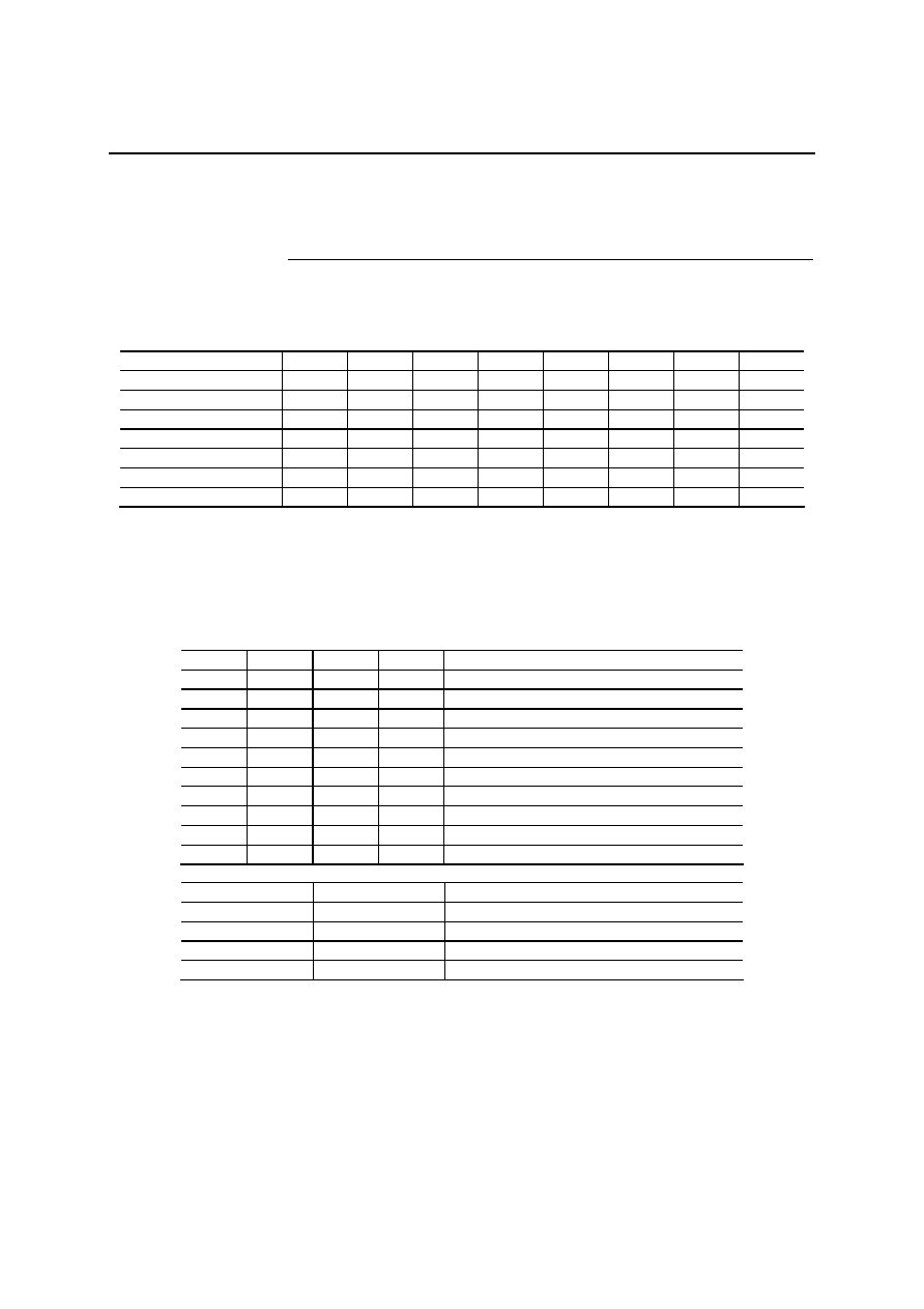
CVOL Command
The CVOL command adjusts the volume of the specified channel to the volume which corresponds to the size of
data stored in the TMP register at the rise of the
WR pulse.
Volume can be set in 16 steps up to 30 dB in 2dB step units. Set data as shown in Table 7.
Table 7 Volume Setting Data Configuration
D3 D2 D1 D0
Volume(dB)
0 0 0 0
0
dB
0 0 0 1
2
dB
0 0 1 0
4
dB
0 0 1 1
6
dB
0 1 0 0
8
dB
0 1 0 1
10
dB
0 1 1 0
12
dB
0 1 1 1
14
dB
1 0 0 0
16
dB
1 0 0 1
18
dB
1 0 1 0
20
dB
1 0 1 1
22
dB
1 1 0 0
24
dB
1 1 0 1
26
dB
1 1 1 0
28
dB
1 1 1 1
30
dB
(D7-D4: Don't care)
When power is turned on and the
RESET pulse is input, all channels are set to 0dB.

FEDL9811FULL-04
OKI Semiconductor
MSM9811
36/44
PAN Command
The PAN command adjusts the volume of the specified channel for the left and right respectively, to the volume
which corresponds to the size of data stored in the TMP register at the rise of the
WR pulse.
This command enables stereo output.
When volume is controlled by the OPT command and CVOL command, volume to be output is the volume stored
in ROM multiplied by volume set by the OPT command, CVOL command, and PAN command respectively. This
volume is output from LDAO and RDAO.
Volume can be set in 16 steps up to 30 dB in 2 dB step units. Set data as shown in Table 8.
Table 8 PAN Data Configuration
D7 D6 D5 D4 Volume
at
left
side
D3 D2 D1 D0 Volume
at
right
side
0 0 0 0
0
dB
0 0 0 1
2
dB
0 0 1 0
4
dB
0 0 1 1
6
dB
0 1 0 0
8
dB
0 1 0 1
10
dB
0 1 1 0
12
dB
0 1 1 1
14
dB
1 0 0 0
16
dB
1 0 0 1
18
dB
1 0 1 0
20
dB
1 0 1 1
22
dB
1 1 0 0
24
dB
1 1 0 1
26
dB
1 1 1 0
28
dB
1 1 1 1
30
dB

FEDL9811FULL-04
OKI Semiconductor
MSM9811
37/44
FLOWCHART
Monaural Playback
Select a phrase to start voice synthesis.
(FADR command)
Start monaural playback.
Set up PAN for each channel.
(PAN command)
End playback?
Select a channel to end playback.
(STOP command)
Yes
No
Select a channel to start playback.
(START command)
Do mixing with other channels?
Set up a volume for each channel.
(CVOL command)

FEDL9811FULL-04
OKI Semiconductor
MSM9811
38/44
Stereo Playback
Select a phrase of a left side channel.
(FADR command)
Start stereo playback.
Do mixing with other channels?
Start playback.
(START command)
End playback?
Select a channel to end playback.
(STOP command)
No
Yes
Select a phrase of a right side channel.
(FADR command)
Set up PAN of a left side channel.
(PAN command)
Set up PAN of a right side channel.
(PAN command)

FEDL9811FULL-04
OKI Semiconductor
MSM9811
39/44
Continuous Playback
Select a phrase to start voice synthesis.
(FADR command)
Start continuous playback.
Set up PAN.
(PAN command)
Select a channel to start playback.
(START command)
Start voice synthesis of the first
phrase.
NCR = 1?
Select a phrase to be played next.
(FADR command)
Select a channel to start playback.
(START command)
Select a phrase to be played next.
No
Yes
Set up CVOL.
(CVOL command)
Is it possible to select a phrase
to be played next?

FEDL9811FULL-04
OKI Semiconductor
MSM9811
40/44
Changing Volume Level
It is possible to change the volume level of a channel that is being played. If the CVOL command is issued when
voices are not being played, the changed volume level will be valid during the next playback. When the phrase
control table function is used, the value of CVOL is changed by the phrase control table function because there are
volume setting values in the phrase control table.
CVOL command
Voices are being played
(BUSY = 0)
Change the volume level of the
selected channel?
Yes
No
PAN command
Change the volume level of the
selected channel.
Yes
No
Change the volume level of the
selected channel.
Change PAN of the channel?

FEDL9811FULL-04
OKI Semiconductor
MSM9811
41/44
APPLICATION CIRCUITS
19
8
MCU
M
9811
RA2
0
RA1
9
R
A
18-0
RD7
-0
SD
SI
SO
C
MD CS WR RD RES
E
T
SERIAL
NCR/
BU
S
Y
R
CS
TE
S
T
1
TE
S
T
2
TE
S
T
3
TE
S
T
4
R
O
E
LD
AO
CE
A
18-0
D7
-0
CE
A
18-0
D7
-0
CE
A
18-0
D7
-0
CE
A
18-0
D7
-0
OE
OE
OE
OE
2B
2A
Y3
Y2
Y1 Y0
1
G
2G
74H
C
139
M
S
M
27C401CZ
M
S
M
27C401CZ
M
S
M
27C401CZ
M
S
M
27C401CZ
XT
XT
AM
P
A
p
pli
cation ci
rcuit
exampl
e w
h
en four 4 M
b
it O
T
P
RO
M
s
are conne
cted (se
r
ial input inte
rfac
e)
RDAO
AM
P

FEDL9811FULL-04
OKI Semiconductor
MSM9811
42/44
PACKAGE DIMENSIONS
(Unit: mm)
QFP64-P-1414-0.80-BK
Mirror finish
Package material
Epoxy resin
Lead frame material
42 alloy
Pin treatment
Solder plating (
5µm)
Package weight (g)
0.87 TYP.
5
Rev. No./Last Revised
6/Feb. 23, 2001
Notes for Mounting the Surface Mount Type Package
The surface mount type packages are very susceptible to heat in reflow mounting and humidity absorbed in
storage.
Therefore, before you perform reflow mounting, contact Oki's responsible sales person for the product name,
package name, pin number, package code and desired mounting conditions (reflow method, temperature and
times).

FEDL9811FULL-04
OKI Semiconductor
MSM9811
43/44
REVISION HISTORY
Page
Document
No.
Date
Previous
Edition
Current
Edition
Description
FEDL9811FULL-01
Jun. 2000
Edition 1
FEDL9811FULL-02
May. 2001
Edition 2
7,20,31,32
7,20,31,32
Corrected t
he output impedance of analog
signals
.
FEDL9811FULL-03
Jun 20, 2003
7 7
Corrected the word "AOUT" to "LDAO,RDAO"
In Analog Characteristics table.
FEDL9811FULL-04
Sep. 1, 2004
Edition 4

FEDL9811FULL-04
OKI Semiconductor
MSM9811
44/44
NOTICE
1. The information contained herein can change without notice owing to product and/or technical improvements.
Before using the product, please make sure that the information being referred to is up-to-date.
2. The outline of action and examples for application circuits described herein have been chosen as an explanation
for the standard action and performance of the product. When planning to use the product, please ensure that the
external conditions are reflected in the actual circuit, assembly, and program designs.
3. When designing your product, please use our product below the specified maximum ratings and within the
specified operating ranges including, but not limited to, operating voltage, power dissipation, and operating
temperature.
4. Oki assumes no responsibility or liability whatsoever for any failure or unusual or unexpected operation
resulting from misuse, neglect, improper installation, repair, alteration or accident, improper handling, or
unusual physical or electrical stress including, but not limited to, exposure to parameters beyond the specified
maximum ratings or operation outside the specified operating range.
5. Neither indemnity against nor license of a third party's industrial and intellectual property right, etc. is granted
by us in connection with the use of the product and/or the information and drawings contained herein. No
responsibility is assumed by us for any infringement of a third party's right which may result from the use
thereof.
6. The products listed in this document are intended for use in general electronics equipment for commercial
applications (e.g., office automation, communication equipment, measurement equipment, consumer
electronics, etc.). These products are not, unless specifically authorized by Oki, authorized for use in any
system or application that requires special or enhanced quality and reliability characteristics nor in any system
or application where the failure of such system or application may result in the loss or damage of property, or
death or injury to humans.
Such applications include, but are not limited to, traffic and automotive equipment, safety devices, aerospace
equipment, nuclear power control, medical equipment, and life-support systems.
7. Certain products in this document may need government approval before they can be exported to particular
countries. The purchaser assumes the responsibility of determining the legality of export of these products and
will take appropriate and necessary steps at their own expense for these.
8. No part of the contents contained herein may be reprinted or reproduced without our prior permission.
Copyright 2004 Oki Electric Industry Co., Ltd.