
FEDL60852A-03
1Semiconductor
This version: Nov. 2001
Previous version: Oct. 2001
ML60852A
USB Device Controller
1/81
GENERAL DESCRIPTION
The ML60852A is a general purpose Universal Serial Bus (USB) device controller.
The ML60852A provides a USB serial interface engine, USB transceiver, FIFOs, control/status registers,
application interface circuit, and oscillation circuit thereby easily realizing a USB system. The ML60852A
supports four types of data transfer such as control transfer, bulk transfer, interrupt transfer and isochronous
transfer, and also supports five or six endpoints.
FEATURES
�
USB1.1 compliant
�
Supports full-speed (12 Mbps).
�
Supports four types of transfer; control transfer, bulk transfer, interrupt transfer, and isochronous transfer.
�
Endpoints: 5 to 6 endpoints
Control EP
1
Bulk/interrupt EP
3
Isochronous/bulk/interrupt EP
1 or 2
�
Built-in FIFO for data storage
�
A two-layer configuration of FIFO for each of EP1, EP2, EP4, and EP5
�
8/16 bit DMA supported (EP1, EP2, EP4, and EP5)
�
Intelligent Serial Interface Engine (SIE)
�
Supports bus-powered device.
The suspend condition is automatically detected and the low-power mode is activated. Normal operation is
automatically restarted when the resume condition is detected.
�
Built-in USB transceiver circuit
�
Ta = -20 to +80 �C
�
V
CC
=3.0 to 3.6 V
�
Interface with 5 V circuit is possible. (Input: 5 V tolerant, output: TTL)
�
Built-in 12 MHz /6 MHz oscillation circuit
�
Package options:
44-pin plastic TQFP
56-pin plastic LGA
FEDL60852A-03
1Semiconductor
ML60852A
2/81
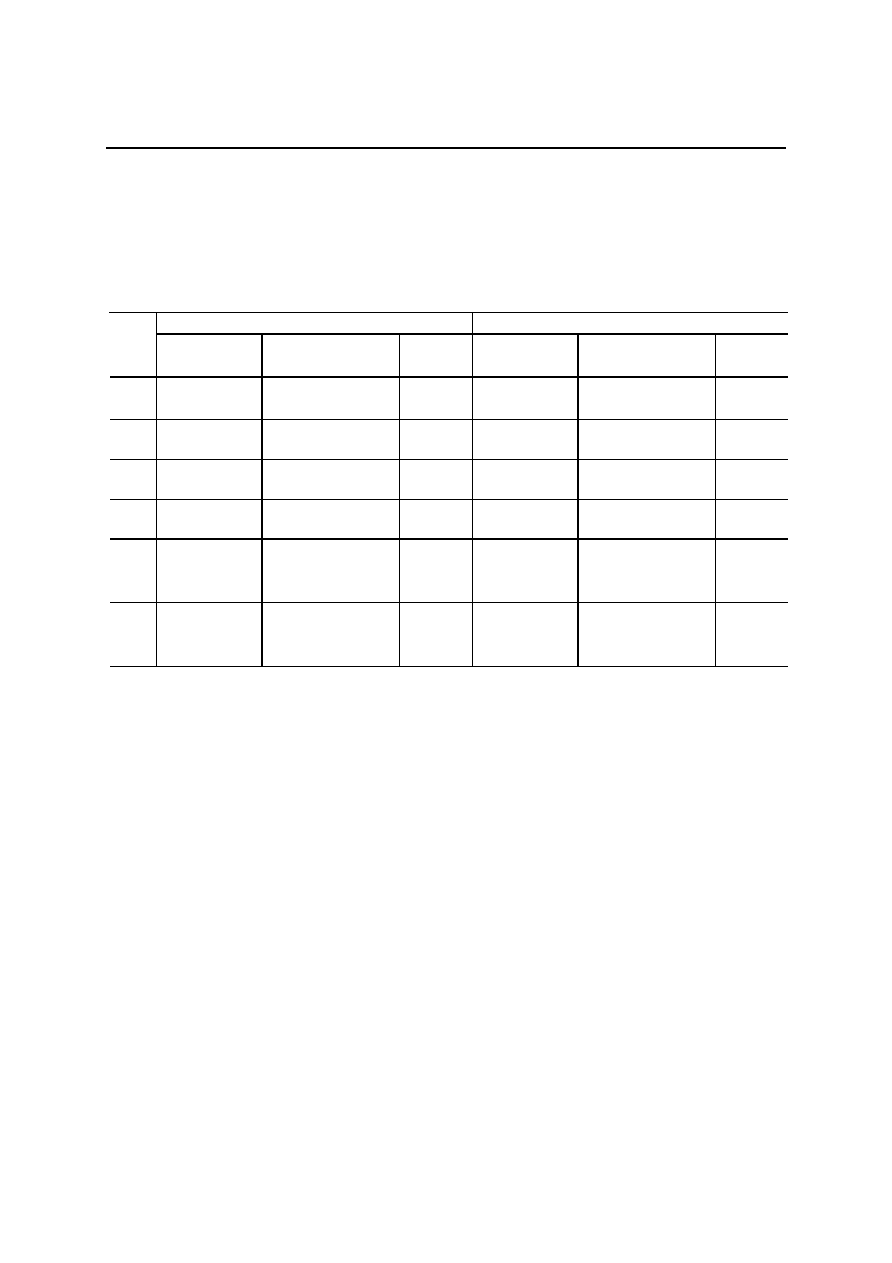
Endpoints and FIFOs
By initializing appropriate registers, the ML60852A can be operated in either 5EP or 6EP mode. Although the
transfer mode that can be used by EP0 is fixed, it is possible to select either the bulk transfer mode or the interrupt
transfer mode for end points EP1, EP2, and EP3, and one of the modes of isochronous, bulk, or interrupt transfer
can be selected for EP4 and EP5. In addition, it is possible to selectively set the direction of data transfer for EP1 to
EP5.
5EP Mode
6EP Mode
End
point
FIFO
Capacity
Transfer
mode
Remarks
FIFO
Capacity
Transfer
mode
Remarks
EP0
Reception 32
Transmission 32
Control transfer
Reception 32
Transmission 32
Control transfer
EP1
64x2
Bulk/interrupt transfer
(IN/OUT)
DMA
Possible
64x2
Bulk/interrupt transfer
(IN/OUT)
DMA
Possible
EP2
64x2
Bulk/interrupt transfer
(IN/OUT)
DMA
Possible
64x2
Bulk/interrupt transfer
(IN/OUT)
DMA
Possible
EP3
32
Bulk/interrupt transfer
(IN/OUT)
32
Bulk/interrupt transfer
(IN/OUT)
EP4
512x2
(64x2)
Isochronous/bulk/
interrupt transfer
(IN/OUT)
DMA
Possible
256x2 (64x2)
Isochronous/bulk/
interrupt transfer
(IN/OUT)
DMA
Possible
EP5
--
--
256x2 (64x2)
Isochronous/bulk/
interrupt transfer
(IN/OUT)
DMA
Possible
FIFO Capacity: The unit is bytes.
Note 1: The selection between the 5EP mode and the 6EP mode is made by bit D2 of the register
SYSCON.
Note 2: EP3 permits rate feedback data sequence toggling.
Note 3: EP1, EP2, and EP3 are all mutually independent, and can be assigned for bulk transfer or
interrupt transfer individually. It is possible to set the maximum packet size up to 64 bytes (32
bytes for EP3) during both bulk transfer and interrupt transfer.
Note 4: It is possible to set EP4 and EP5 to one of the modes of isochronous transfer, bulk transfer, and
interrupt transfer. The maximum packet size can be up to 64 bytes when these end points are set
to bulk transfer.
Note 5: When using EP4 and EP5 in the isochronous transfer mode:
In the 5EP mode, the maximum packet size of EP4 is 512 bytes. EP5 cannot be used.
In the 6EP mode, the maximum packet size of both EP4 and EP5 is 256 bytes.

FEDL60852A-03
1Semiconductor
ML60852A
5/81
PIN DESCRIPTION
Pin name
Pin count
I/O
Description
D+, D-
2
I/O
USB data
XIN, XOUT
2
--
Pins for external crystal
AD7:AD0
8
I/O
Data bus (LSB)/address inputs
A6:A0
7
I
Address inputs
D15:D8
8
I/O
Data bus (MSB)
CS
1
I
Chip select signal input pin. Active "L"
RD
1
I
Read signal input pin. Active "L"
WR
1
I
Write signal input pin. Active "L"
INTR
1
O
Interrupt request signal output pin
DREQ0
1
O
DMA0 request output pin
DREQ1
1
O
DMA1 request output pin
DACK0
1
I
DMA0 reception signal input pin
DACK1
1
I
DMA1 reception signal input pin
ALE/PUCTL
1
I,O
Address latch enable signal input pin/pull-up control pin
ADSEL
1
I
Address input format select input pin
RESET
1
I
Reset signal input pin
TEST1, TEST2
2
I
Test pin. (Normally at "L")
V
CC
2
3.3 V power supply pin
GND
2
GND
44