OKI Semiconductor
FEDW9041BB-02
Issue Date: May 20. 2002
MBF9041BB
SAW Antenna Duplexer (700 to 1000 MHz)
1/11
GENERAL DESCRIPTION
The MBF9041BB is the SAW antenna duplexer for the frequency range of 700 to 1000 MHz.
This SAW Duplexer integrates RF filters at Tx and Rx side, and matching circuit into PKG. This helps to save the
space and weight greatly in the target application such as mobile telephone.
This SAW Duplexer has very low insertion loss by using high quality package.
Due to high harmonics characteristics, total number of components at RF circuit can be minimized.
Thanks to high isolation performance, high sensitivity can be expected. Low insertion loss at Tx saves the power
consumption of mobile telephone which prolong the battery life.
FEATURES
�
Complying Standard AMPS, IS-95, IS-136
�
Thin package: less than 1.5 mm in height
�
PKG I/O Impedance: 50
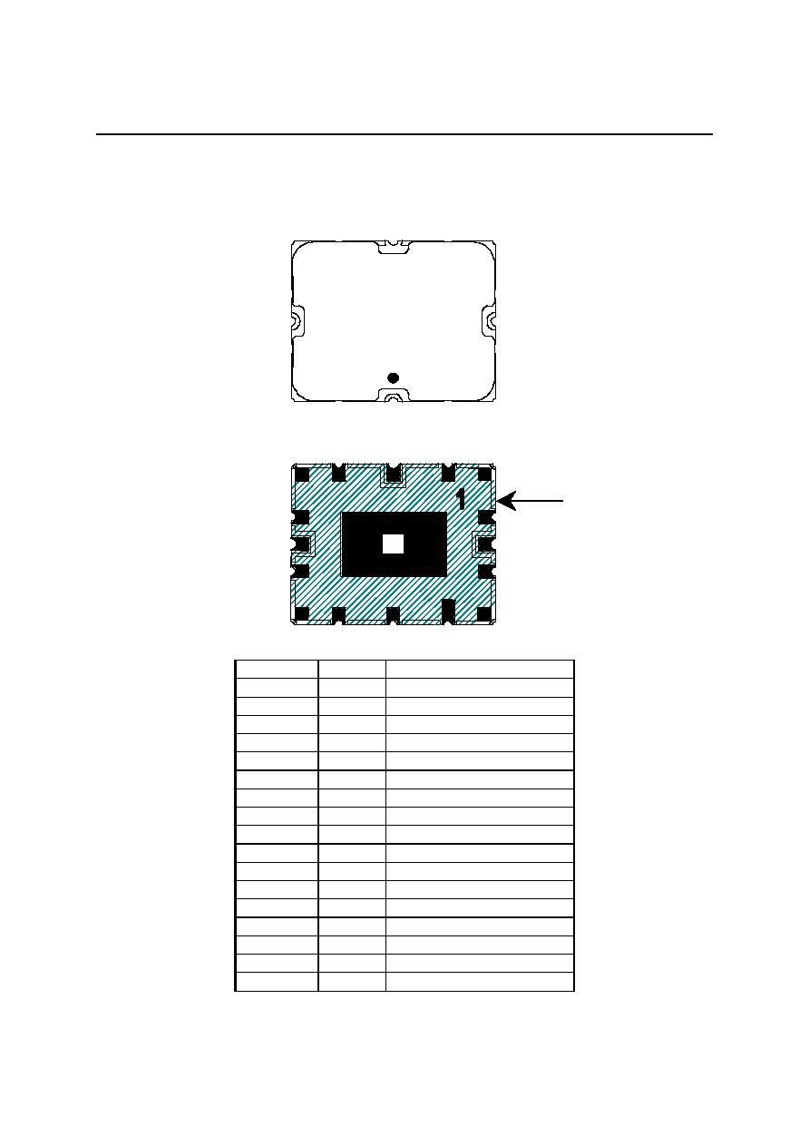
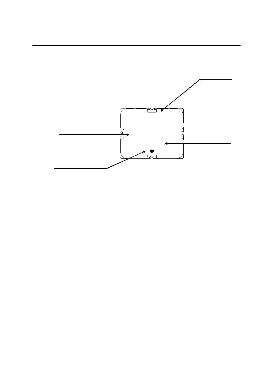
PRODUCT DESCRIPTION
Package Type
MBF9041BB
OKI
041BB
YZZZ
ANT
Rx
Tx
FEDW9041BB-02
OKI Semiconductor
MBF9041BB
9/11
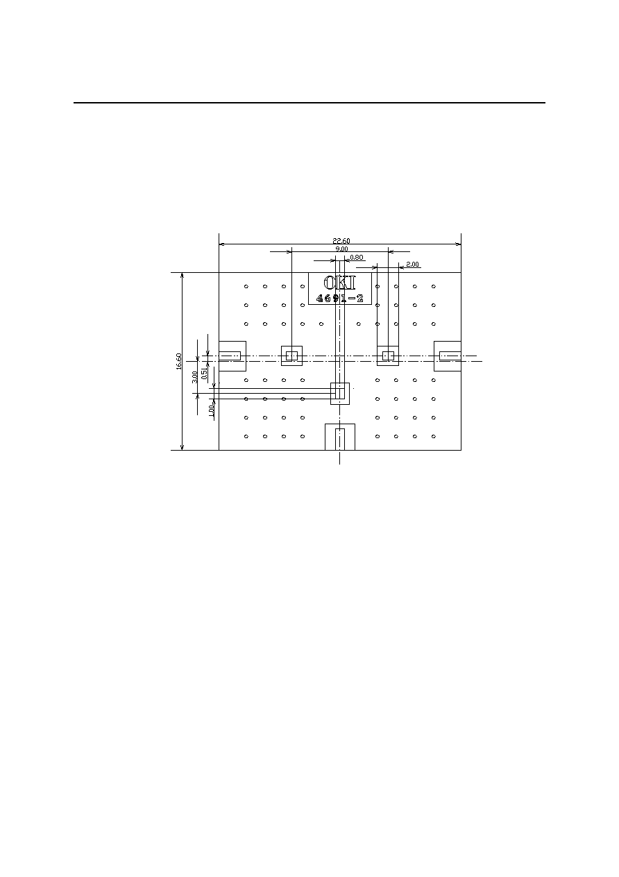
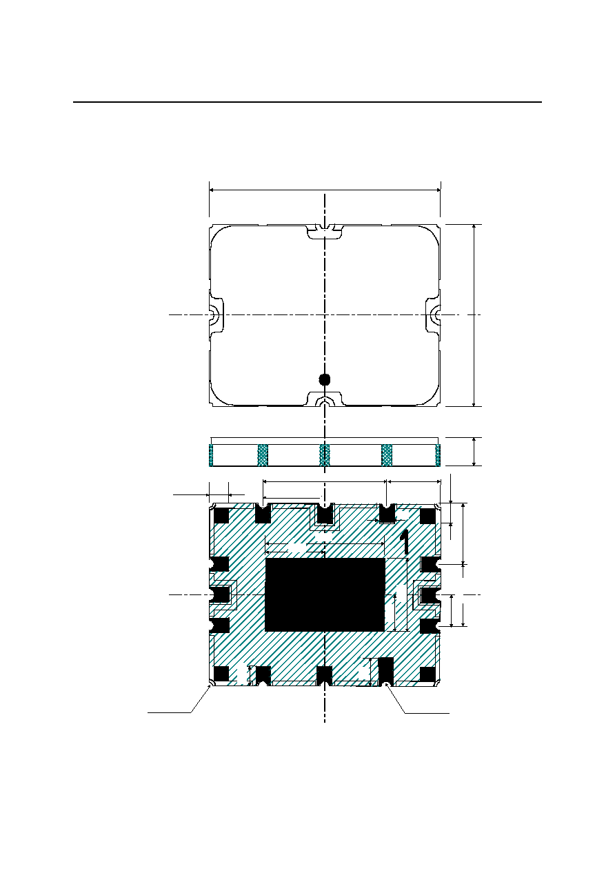
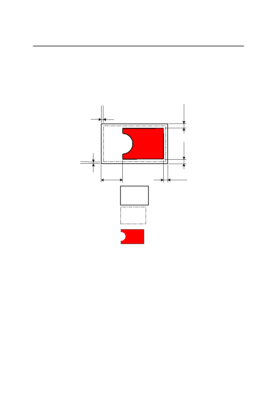
RECOMMENDATION FOR SOLDER PAD PATTERN
The solder pad pattern should be designed by customers because it depends on the electrical
performance of the customers' system. Following is an example of solder pad pattern which is used in
OKI's package evaluation board. Please be noted that this is for reference purpose only.
0.1 mm
0.1 mm
0.5 mm
PCB pad pattern
Metal mask pattern
0.1 mm
25
�
m
25
�
m
Pad of Device
Please pay attention to the following items to maintain electrical performance.
(1) Metal mask pattern for cream solder should be 25
�
m smaller on each side. Metal mask is 0.15 mm in
thickness.
(2) As the impedance of Tx, Rx, ANT is designed for 50
, please consider this for the design of mother board.
(3) The performance of these devices is assured when GND pad (Pin 17) is connected. GND pad (Pin 17) should
be soldered in the same way as above.

FEDW9041BB-02
OKI Semiconductor
MBF9041BB
11/11
NOTICE
1. The information contained herein can change without notice owing to product and/or technical improvements.
Before using the product, please make sure that the information being referred to is up-to-date.
2. The outline of action and examples for application circuits described herein have been chosen as an
explanation for the standard action and performance of the product. When planning to use the product, please
ensure that the external conditions are reflected in the actual circuit, assembly, and program designs.
3. When designing your product, please use our product below the specified maximum ratings and within the
specified operating ranges including, but not limited to, operating voltage, power dissipation, and operating
temperature.
4. Oki assumes no responsibility or liability whatsoever for any failure or unusual or unexpected operation
resulting from misuse, neglect, improper installation, repair, alteration or accident, improper handling, or
unusual physical or electrical stress including, but not limited to, exposure to parameters beyond the specified
maximum ratings or operation outside the specified operating range.
5. Neither indemnity against nor license of a third party's industrial and intellectual property right, etc. is
granted by us in connection with the use of the product and/or the information and drawings contained herein.
No responsibility is assumed by us for any infringement of a third party's right which may result from the use
thereof.
6. The products listed in this document are intended for use in general electronics equipment for commercial
applications (e.g., office automation, communication equipment, measurement equipment, consumer
electronics, etc.). These products are not authorized for use in any system or application that requires special
or enhanced quality and reliability characteristics nor in any system or application where the failure of such
system or application may result in the loss or damage of property, or death or injury to humans.
Such applications include, but are not limited to, traffic and automotive equipment, safety devices, aerospace
equipment, nuclear power control, medical equipment, and life-support systems.
7. Certain products in this document may need government approval before they can be exported to particular
countries. The purchaser assumes the responsibility of determining the legality of export of these products
and will take appropriate and necessary steps at their own expense for these.
8.
No part of the contents contained herein may be reprinted or reproduced without our prior permission.
Copyright 2002 Oki Electric Industry Co., Ltd.