Target Specification
Preliminary
Oki Electric Industry Co.,Ltd.
No.
GTD-18414 rev.1
1
/5
Electronic Components
KGL4225D 14-Gbps 1:16 MUX
.
1. DESCRIPTION
KGL 4225D converts 16bit parallel data into one data stream operating over 14GHz clock frequency.
The KGL 4225D is fabricated by OKI 0.18
µ
m gate length GaAs MESFETs process. By using of OKI unique
flip-flops, which are MCFF (Memory Cell type Flip Flop), high speed operation has been realized. Capacitive
coupling is recommended for clock input connection. The data output level is compatible with SCFL. Low
speed signal interfaces are compatible with ECL. The device is mounted in 48pin package.
2. ABSOLUTE MAXIMUM RATINGS
No.
Item
Symbol Min. Max. Unit
1 Supply Voltage
VTT
-2.3
0.3
V
2 Clock and Data Input Voltage
VCDI
-2.3
-0.5
V
3 Package Base Temperature under Bias
Ts
-45
100
°
C
4 Storage Temperature
Tst
-45
125
°
C
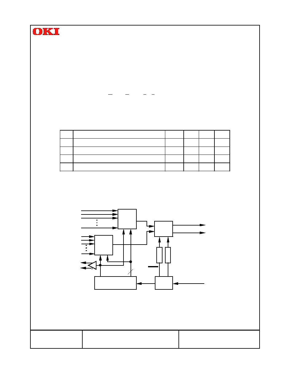
3. FUNCTIONAL BLOCK DIAGRAM
1/2
divider
8:1
MUX
8:1
MUX
controller
2:1
MUX
Figure 1 Block Diagram of KGL4225D
D0
D2
D4
DE
1/2CK
delay
1/2CK
HCK
Q
QN
D1
D3
D5
DF
LCK
LCKN
delay
1/2CK
8
control pulses
1/16CK

Target Specification
Preliminary
Oki Electric Industry Co.,Ltd.
No.
GTD-18414 rev.1
2
/5
4. RECOMMENDED OPERATING CONDITIONS
Item
Symbol
Min. Typ. Max. Unit
Power Supply
VTT
-2.1
-2.0
-1.9
V
Operating Temperature Range at Package Base
Ts
0
70
°
C
5. ELECTRICAL CHARACTERISTICS
5-1 AC CHARACTERISTICS
VTT=-2V
±
0.1V, Ts = 0~70
°
C
Item
Symbol
Test Condition
Min.
Typ.
Max. Unit
Clock Period
t
C
71
---
---
ps
Set-up time (D0
F to LCK
)
t
DS
Input clock period : 71ps.
TBD
930
TBD
ps
Hold time (LCK
to D0
F)
t
DH
Input clock period : 71ps.
TBD
-690
TBD
ps
HCK-D0
F Phase Margin
t
M
Input clock period : 71ps.
TBD
816
---
ps
Rise Time (Q, QN) 20%-80%
tr
Input clock period : 71ps.
---
25
TBD
ps
Fall Time (Q, QN) 20%-80%
tf
Input clock period : 71ps.
---
25
TBD
ps
Valid
Valid
t
M
t
DS
t
C
HCK
D0
~DF
LCK
LCKN
t
DH
Figure 2 Waveforms of KGL4225D
Target Specification
Preliminary
Oki Electric Industry Co.,Ltd.
No.
GTD-18414 rev.1
3
/5
100%
80%
20%
0%
Figure 3 Rise and Fall Time
tr
tf
C1
I1
K1
M1
O1
A2
C2
J1
L1
N1
P1
B2
C3
E3
D3
B3
A3
P2
O2
Figure 4 Time Chart of KGL4225D
HCK
D0
D1
D2
D3
D4
DE
DF
Q
QN
LCKN
LCK
A1
B1
D1
E1
O1
P1
P3
O3
C2
E2
D2
B2
A2
I1
K1
M1
O1
A2
C2
J1
L1
N1
P1
B2
Target Specification
Preliminary
Oki Electric Industry Co.,Ltd.
No.
GTD-18414 rev.1
4
/5
5.2
DC CHARATERISTICS
VTT=-2V
±
0.1V, Ts = 0
70
°
C
Item
Symbol
Test Condition
Min. Typ. Max. Unit
Power Dissipation
PW
---
3.0
4.0
W
Clock Input Voltage Swing (HCK)
VCKI
AC Coupling
T B D
1.0
T B D
Vpp
Low level of Data Input (D0
DF)
VDIL
-2.1
-1.7
-1.55
V
High level of Data Input (D0 ~DF)
VDIH
-1.16
-1.0
-0.65
V
Low Level of Data Output (Q, QN)
VDOL
50
to GND
T B D -0.15 T B D
V
High Level of Data Output (Q, QN)
VDOH
50
to GND
T B D
-0.9
T B D
V
Low level of 1/16CK Output (LCN, LCKN)
VCOL
50
to VTT
-1.95
-1.8
-1.55
V
High level of 1/16CK Output (LCN, LCKN)
VCOH
50
to VTT
-1.15 -0.93 -0.75
V
6.
PIN ASSIGNMENT
1
2
3
4
5
6
7
8
9
10
11
12
48
47
46
45
44
43
42
41
40
39
38
37
36
35
34
33
32
31
30
29
28
27
26
25
13 14
15
16
17
18
19
20
21
22
23
24
VTT
D1
D3
D5
D7
VTT
G
D9
DB
DD
DF
VTT
VTT
D0
D2
D4
D6
G
VTT
D8
DA DC
DE
VTT
G
LCKN
G
LCK
G
VTT
VTT
G
Q
G
QN
G
G
G
G
G
G
VTT
VTT
G
HCK
G
HCR
G
(Top View)
Note: 1.
G is a ground terminal.
2 . H C R i s a c l o c k r e f e r e n c e t e r m i n a l . U s u a l l y H C R i s
connected to VTT t h r o u g h a c a p a c i t o r ( 1 0 0 n F )
Figure 5 PIN Assignment of KGL4225D
Target Specification
Preliminary
Oki Electric Industry Co.,Ltd.
No.
GTD-18414 rev.1
5
/5
7.
PACKAGE DIMENSIONS
37
13.97
unit : mm
17.41 SQ.
15.57 SQ.
12.00 SQ.
13
25
1
1.80
0.7
0.5
0.60
2
±
0.3
0.125
±
0.05
Figure 6 48pin Package Dimensions
0.40
±
0.05
1.27
8. TYPICAL INTERFACE CONFIGURATION
VDIH=-1.1V,VDIL=-1.6V
Zo=50
14
Zo=50
38
Zo=50
28
D0
50
50
DF
HCK
G
1,3,5,8,10,12,18,
25,27,29,32,33,34,
35,36,42
VTT
VTT
VTT
VTT
VTT
VTT
-2V
6,7,13,19,
24,30,31,
37,43,48
Q
LCK
9
11
4
2
Zo=50
Zo=50
Zo=50
Zo=50
50
50
50
50
QN
LCKN
Figure 7 Typical Interfacing Configuration of KGL4225D
50
VCKI=0.7Vpp
VCOH=-0.93V,VCOL=-1.8V
26
100nF
HCR
KGL4225D