1
Oki Semiconductor
KGL4203
10-Gbps GaAs EXOR/NOR IC
INTRODUCTION
Oki Semiconductor's KGL4203 is a 10-Gbps GaAs EXOR/NOR IC designed for ultra high-speed digital
communications systems. The KGL4203 uses 0.2-µm gate length GaAs MESFETs and Oki's unique DCFL
( Direct Coupled FET Logic ) technology to achieve operations of 10-GHz or more. The KGL4203 is
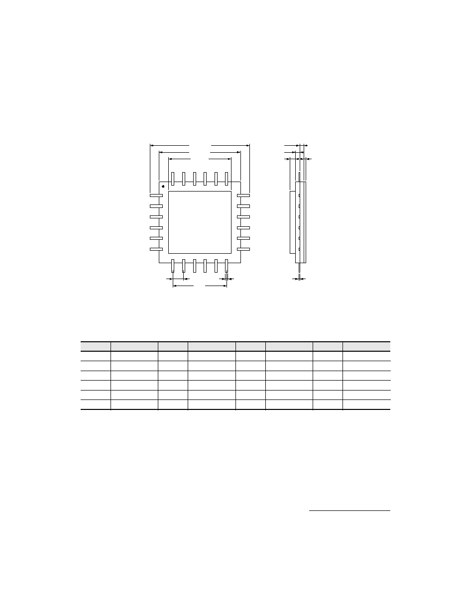
available as a 24-pin ceramic packaged device. Due to the KGL4203's high sensitivity, capacitive
coupling is recommended for the interface.
FEATURES
· High-speed operation: 10-Gbps data rate (min)
· High sensitivity: 50 to 600 mV
PP
(at 10 Gbps 2
23
-1 PRPS, capacitive coupling)
· Low-power dissipation: 540 mW (typ.) using 2-V power-supply
· 0.2-µm gate length GaAs MESFET process
· DCFL (Direct Coupled FET Logic) technology
· 24-pin ceramic package
APPLICATION
· High-speed optical communication systems: 10 Gbps
· High-speed test equipment
s
KGL4203
s
2
Oki Semiconductor
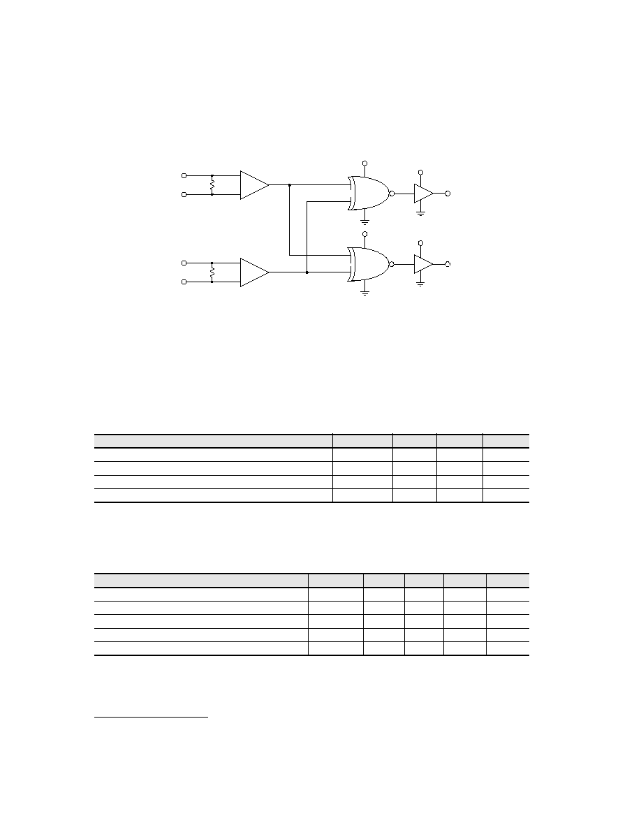
BLOCK DIAGRAM
ELECTRICAL CHARACTERISTICS
Exceeding these maximum ratings could cause immediate damage or lead to permanent deterioration of the device.
Absolute Maximum Ratings
Parameter
Symbol
Min.
Max.
Units
Supply Voltage
V
DD
-0.3
2.3
V
Data Input Voltage ( D1, D2 )
V
DI
-0.3
1.5
V
Temperature at Package Base Under Bias
Ts
-45
100
°C
Storage Temperature
Tst
-45
125
°C
Electrical Characteristics
V
DD
= 2 V ± 0.1 V, Ts = 0°C to 70°C
Parameter
Symbol
Min.
Typ.
Max.
Units
Maximum Operating Data Bit Rate
DAR
10
Gbps
Power Dissipation
PW
0.54
0.68
W
Data Input Voltage Swing ( D1, D2 )
D
IS
0.5
0.9
Vpp
Data Output Voltage Swing ( Q, QN )
D
OS
0.8
1.0
1.2
Vpp
Output ( Q, QN ) Rise Time and Fall Time
T
RF
30
40
ps
QN
V
DD
D1R
D1
50
D2R
D2
50
Q
V
DD
V
DD
V
DD
D1, D2
Data Input Terminals
D1R, D2R
Reference Voltage Terminals. Usually D1R and D2R are connected to ground through a capacitor (0.1 µF).
Q, QN
Complimentary Data Outputs
VDD
Power Supply of Internal Circuit