PRODUCT SPECIFICATION
Nordic VLSI ASA - Vestre Rosten 81, N-7075 Tiller, Norway - Phone +4772898900 - Fax +4772898989
Revision: 2.1
Page 1 of 16
February 2000
433MHz Single Chip RF Transmitter
FEATURES
·
True single chip FSK transmitter
·
Few external components required
·
On chip UHF synthesiser
·
No set up or configuration
·
20kbit/s data rate
·
2 channels
·
Very low power consumption
·
Standby mode
APPLICATIONS
·
Alarm Systems
·
Automatic Meter Reading (AMR)
·
Keyless entry
·
Home Automation
·
Remote Control
·
Surveillance
·
Automotive
·
Telemetry
·
Toys
·
Wireless Communication
GENERAL DESCRIPTION
nRF402 is a true single chip UHF transmitter designed to operate in the 433MHz ISM
(Industrial, Scientific and Medical) frequency band. It features Frequency Shift
Keying (FSK) modulation capability. nRF402 operates at data rates up to 20kbits/s.
Transmit power can be adjusted to a maximum of +10dBm. Antenna interface is
differential and suited for low cost PCB antennas. nRF402 operates from a single 3V
DC supply and has a standby mode which makes power saving easy and efficient.
As a primary application, nRF402 is intended for UHF radio equipment in compliance
with the European Telecommunication Standard Institute (ETSI) specification
EN 300 220-1 V1.2.1.
QUICK REFERENCE DATA
Parameter
Value
Unit
Frequency, Channel#1/Channel#2
433.92 / 434.33
MHz
Modulation
FSK
Frequency deviation
±
15
kHz
Max. RF output power @ 400
, 3V
10
dBm
Maximum bit rate
20
kbit/s
Supply voltage
2.7 3.6
V
Transmit supply current @ -10 dBm RF output power
8
mA
Standby supply current
8
µ
A
Table 1. nRF402 quick reference data
ORDERING INFORMATION
Type number
Description
Version
nRF402-IC
14 pin SSOIC
A
nRF402-EVKIT
Evaluation kit with nRF402 IC
1.0
Table 2. nRF402 ordering information
nRF402
PRODUCT SPECIFICATION
nRF402 Single Chip RF Transmitter
Nordic VLSI ASA Vestre Rosten 81, N-7075 Tiller, Norway - Phone +4772898900 - Fax +4772898989
Revision: 2.1
Page 2 of 16
February 2000
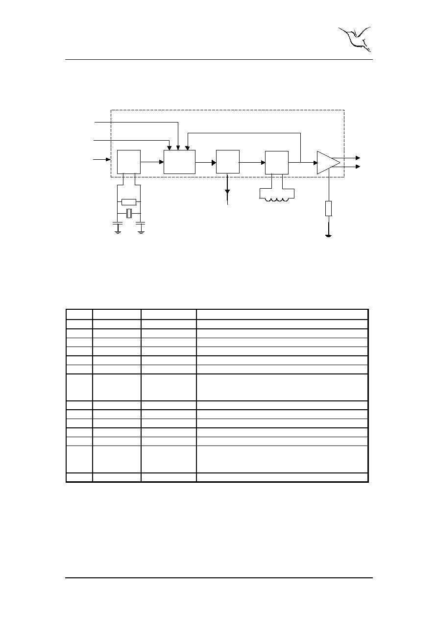
BLOCK DIAGRAM
PLL
OSC
LPF
6
4
1
14
9
DIN
CS
7
PWR_UP
13
PA
VCO
5
8
RF_PWR
LOOP
FILTER
VCO
INDUCTOR
REFERENCE
11
10
ANT1
ANT2
Figure 1. nRF402 block diagram with external components
PIN FUNCTIONS
Pin
Name
Pin function
Description
1
XC1
Input
Crystal oscillator input
2
VSS
Ground
Ground (0V)
3
VDD
Power
Power supply (+3V DC)
4
VCO1
Input
External inductor for VCO
5
VCO2
Input
External inductor for VCO
6
LPF
Test
Loop filter voltage test pin *
7
CS
Input
Channel selection
CS="0"
433.92MHz, (Channel#1)
CS="1"
434.33MHz, (Channel#2)
8
RF_PWR
Input
Transmit power setting
9
DIN
Input
Data input
10
ANT2
Output
Antenna terminal
11
ANT1
Output
Antenna terminal
12
VSS
Ground
Ground (0V)
13
PWR_UP
Input
Power on/off
PWR_UP = "1"
Power up (Transmit mode)
PWR_UP = "0"
Power down (Standby mode)
14
XC2
Output
Crystal oscillator output
Table 3. nRF402 pin functions
*)
This pin is only for test purposes and is intended for use when measuring the loop filter voltage.

PRODUCT SPECIFICATION
nRF402 Single Chip RF Transmitter
Nordic VLSI ASA Vestre Rosten 81, N-7075 Tiller, Norway - Phone +4772898900 - Fax +4772898989
Revision: 2.1
Page 3 of 16
February 2000
ELECTRICAL SPECIFICATIONS
Conditions: VDD = +3V DC, VSS
= 0V, T
A
= -25
°
C to +85
°
C
Symbol
Parameter (condition)
Min.
Typ.
Max.
Units
VDD
Supply voltage
2.7
3
3.6
V
VSS
Ground
0
V
I
DD
Current consumption in transmit mode
@ -10 dBm RF power
8
mA
I
DD
Current consumption in standby mode
8
µ
A
P
RF
Max. RF output power @ 400
load
10
dBm
V
IH
Logic "1" input voltage
0.7
V
DD
V
DD
V
V
IL
Logic "0" input voltage
0
0.3
V
DD
V
I
H
Logic "1" input current (V
I
= VDD)
+20
µ
A
I
L
Logic "0" input current (V
I
= VSS)
-20
µ
A
f
1
Channel#1 frequency
433.92
MHz
f
2
Channel#2 frequency
434.33
MHz
Modulation type
FSK
f
Frequency deviation
±
15
kHz
f
XTAL
Crystal frequency
1)
4.000
MHz
Bit rate
0
20
kbit/s
Z
I
Recommend antenna port differential load
impedance
400
Spurious emission
Compliant with EN 300-220-1 V1.2.1
2)
Table 4. nRF402 electrical specifications
1)
Crystal stability requirement must match the receiver requirement. For use with nRF401, the
crystal frequency stability should be better than ±45 ppm.
2)
With PCB loop antenna or differential to single ended matching network to a 50
antenna.
ABSOLUTE MAXIMUM RATINGS
Supply voltages
VDD .............................. - 0.3V to +6V
VSS ................................................ 0V
Input voltage
V
I
...................... - 0.3V to VDD + 0.3V
Total power dissipation
P
D
(T
A
=85
°
C).......................... 230 mW
Temperatures
Operating Temperature -25
°
C to +85
°
C
Storage Temperature
- 40
°
C to +125
°
C
Note: Stress exceeding one or more of the limiting values may cause permanent
damage to the device.
ATTENTION!
Electrostatic Sensitive Device
Observe Precaution for handling.
PRODUCT SPECIFICATION
nRF402 Single Chip RF Transmitter
Nordic VLSI ASA Vestre Rosten 81, N-7075 Tiller, Norway - Phone +4772898900 - Fax +4772898989
Revision: 2.1
Page 4 of 16
February 2000
PIN ASSIGNMENT
VSS
VDD
XC1
ANT2
VSS
CS
DIN
ANT1
RF_PWR
VCO1
XC2
PWR_UP
8
14
13
11
10
9
12
1
2
3
4
5
6
7
VCO2
LPF
Figure 2. nRF402 pin assignment
PACKAGE OUTLINE
nRF402, 14 pin SSOIC. Dimensions in mm
Package Type
D
E
H
A
A
1
e
b
L
Copl.
14 pin SSOIC
(5.3 mm)
Min
Max
5.90
6.50
5.00
5.60
7.40
8.20
2.00
0.05
0.65
0.22
0.38
0.55
0.95
0.10
0
°
8
°
Figure 3. SSOIC-14 Package outline
nRF402
14 pin SSOIC
A
1
A
L
E H
D
1 2 3
14 13 12
e b
PRODUCT SPECIFICATION
nRF402 Single Chip RF Transmitter
Nordic VLSI ASA Vestre Rosten 81, N-7075 Tiller, Norway - Phone +4772898900 - Fax +4772898989
Revision: 2.1
Page 5 of 16
February 2000
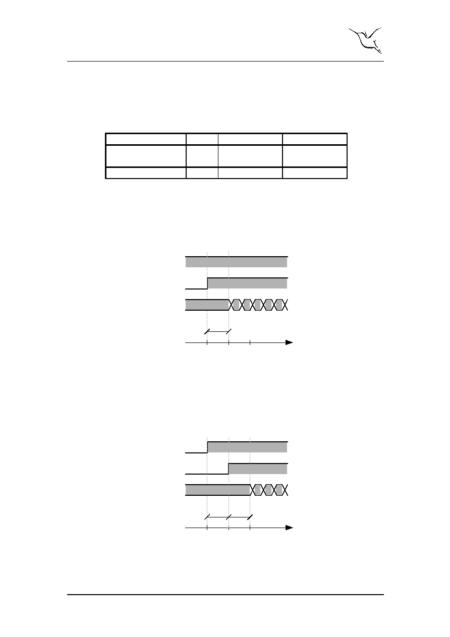
IMPORTANT TIMING DATA
Timing information
The timing information for the different operations is summarised in Table 5.
(TX is transmit mode, Std.by is standby mode.)
Change of Mode
Name
Max Delay
Condition
Std.by
è TX
t
ST
2ms
Operational
mode
V
DD
=0
è TX
t
VT
4ms
Start-up
Table 5 Switching times for nRF402
Switching between standby and TX-mode.
The maximum time from the PWR_UP input is set to "1", until the synthesised
frequency is stable is t
ST
, see Table 5 and Figure 4.
Figure 4 Timing diagram for nRF402 when going from standby to TX-mode
Powering up to transmit-mode (start-up).
Due to spurious emission when the power supply is switched on, the PWR_UP-input
must be kept low for 2ms after VDD > 2.7 V. Data (DIN) is valid within 2ms after
PWR_UP is high.
Figure 5. Timing diagram for nRF402, when powering up to TX-mode
PWR_UP
VDD
Std.by to TX
DIN
0
2
4
ms
2ms
ms
PWR_UP
VDD
VDD=0 to TX
DIN
0
2
4
2ms
2ms