PRODUCT SPECIFICATION
Q5)( *+] 5DGLR 7UDQVPLWWHU ZLWK 0LFURFRQWUROOHU
Nordic VLSI ASA - Vestre Rosten 81, N-7075 Tiller, Norway - Phone +4772898900 - Fax +4772898989
Revision: 1.0
QhtrĂ!ĂsĂ(
August 2003
7$%/( 2) &217(17
1
GENERAL DESCRIPTION....................................................................................4
1.1
Quick Reference Data .......................................................................................4
1.2
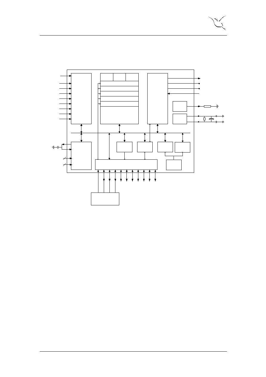
Block Diagram ..................................................................................................5
1.3
Pin Diagram ......................................................................................................6
1.4
Glossary of Terms .............................................................................................8
2
ARCHITECTURAL OVERVIEW..........................................................................9
2.1
Microcontroller .................................................................................................9
2.2
PWM ...............................................................................................................10
2.3
SPI...................................................................................................................10
2.4
Port Logic........................................................................................................10
2.5
Power Management.........................................................................................11
2.6
RTC Wakeup Timer, Watchdog and RC Oscillator .......................................11
2.7
XTAL Oscillator .............................................................................................11
2.8
AD Converter..................................................................................................11
2.9
Radio Transmitter ...........................................................................................12
3
I/O PORTS ............................................................................................................13
3.1
I/O port behavior during RESET ....................................................................13
3.2
Port 0 (P0) .......................................................................................................13
3.3
Port 1 (P1 or SPI port) ....................................................................................14
4
nRF2401 2.4GHz TRANSMITTER SUBSYSTEM .............................................18
4.1
RADIO port (Port 2) .......................................................................................18
4.2
Modes of operation .........................................................................................20
4.3
Device configuration.......................................................................................23
4.4
Data package Description ...............................................................................28
4.5
Important RF Timing Data..............................................................................29
5
A/D CONVERTER ...............................................................................................32
5.1
A/D converter subsystem block diagram ........................................................32
5.2
A/D converter registers ...................................................................................33
5.3
A/D converter usage........................................................................................34
5.4
A/D Converter timing .....................................................................................36
6
PWM......................................................................................................................37
7
INTERRUPTS .......................................................................................................38
7.1
Interrupt SFRs .................................................................................................38
7.2
Interrupt Processing ........................................................................................41
7.3
Interrupt Masking............................................................................................42
7.4
Interrupt Priorities ...........................................................................................42
7.5
Interrupt Sampling ..........................................................................................43
7.6
Interrupt Latency.............................................................................................43
7.7
Interrupt Latency from Power Down State. ....................................................43
7.8
Single-Step Operation .....................................................................................43
8
WAKEUP TIMER AND WATCHDOG...............................................................44
8.1
Tick calibration ...............................................................................................44
8.2
RTC Wakeup timer .........................................................................................44
8.3
Watchdog ........................................................................................................45
8.4
Reset................................................................................................................46

PRODUCT SPECIFICATION
Q5)( *+] 5DGLR 7UDQVPLWWHU ZLWK 0LFURFRQWUROOHU
Nordic VLSI ASA - Vestre Rosten 81, N-7075 Tiller, Norway - Phone +4772898900 - Fax +4772898989
Revision: 1.0
QhtrĂ"ĂsĂ(
August 2003
9
POWER SAVING MODES ..................................................................................47
9.1
Idle Mode ........................................................................................................48
9.2
Stop Mode.......................................................................................................48
9.3
Power down mode...........................................................................................48
10
MICROCONTROLLER.....................................................................................50
10.1 Memory Organization .....................................................................................50
10.2 Program format in external EEPROM ............................................................51
10.3 Instruction Set .................................................................................................52
10.4 Instruction Timing...........................................................................................58
10.5 Dual Data Pointers ..........................................................................................58
10.6 Special Function Registers..............................................................................59
10.7 SFR registers unique to nRF24E2...................................................................62
10.8 Timers/Counters..............................................................................................64
10.9 Serial Interface ................................................................................................72
11
ELECTRICAL SPECIFICATIONS ...................................................................81
12
PACKAGE OUTLINE.......................................................................................83
13
ABSOLUTE MAXIMUM RATINGS ...............................................................84
14
Peripheral RF Information..................................................................................85
15
Table of Figures..................................................................................................86
16
Table of Tables...................................................................................................86
17
DEFINITIONS ...................................................................................................89
PRODUCT SPECIFICATION
Q5)( *+] 5DGLR 7UDQVPLWWHU ZLWK 0LFURFRQWUROOHU
Nordic VLSI ASA - Vestre Rosten 81, N-7075 Tiller, Norway - Phone +4772898900 - Fax +4772898989
Revision: 1.0
QhtrĂ#ĂsĂ(
August 2003
*(1(5$/ '(6&5,37,21
The nRF24E2 is the transmitter part of the nRF2401 2.4GHz radio transceiver plus an
embedded 8051 compatible microcontroller plus a 10-bit 9 input 100 kSPS AD
converter. The circuit is supplied by only one voltage in range 1.9V to 3.6V. The
nRF24E2 supports the proprietary and innovative modes of the nRF2401 such as
ShockBurstTM.
nRF24E2 is also a subset of the nRF24E1 chip, which means that it contains all
functions of nRF24E1 except the radio receive functions, and it also means that it is
fully program compatible with nRF24E1.
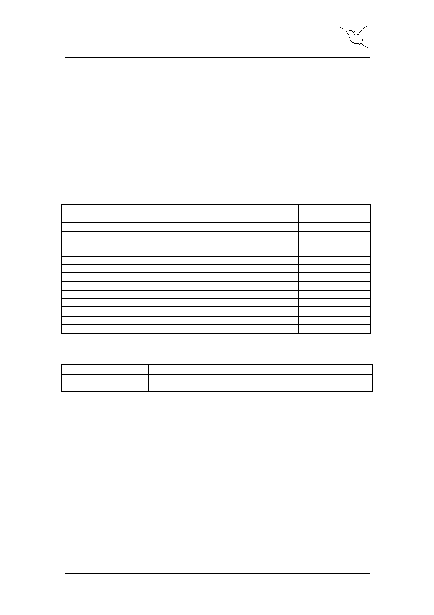
4XLFN 5HIHUHQFH 'DWD
3DUDPHWHU
9DOXH
8QLW
Minimum supply voltage
1.9
V
Temperature range
-40 to +85
°
C
Maximum RF output power
0
dBm
Maximum RF burst data rate
1000
kbps
Supply current for microcontroller @ 16MHz @3V
3
mA
Supply current for ADC @100 kSPS
0.9
mA
Supply current for RF transmit @ -5dBm output power
10.5
mA
Supply current in Power Down mode
2
µ
max CPU clock frequency
20
MHz
max AD conversion rate
100
kSPS
ADC Differential nonlinearity (DNL)
±0.5
LSB
ADC Integral nonlinearity (INL)
±
0.75
LSB
ADC Spurious free dynamic range (SFDR)
65
dB
Package
36 pin QFN 6x6
Table 1-1 : nRF24E2 quick reference data
7\SH 1XPEHU
'HVFULSWLRQ
9HUVLRQ
NRF24E2 IC
36 pin QFN 6x6
A
NRF24E1-EVKIT
Evaluation kit TBD
1.0
Table 1-2 : nRF24E2 ordering information