NTE3881
Integrated Circuit
NMOS, Parallel I/O Interface (PIO), 4MHz
Description:
The NTE3881 Parallel I/O Circuit (PIO) is a programmable, two port device which provides a TTL
compatible interface between peripheral devices and the NTE3880. The Central Processing Unit
(CPU) can configure the NTE3881 to interface with a wide range of peripheral devices with no other
external logic required. Typical peripheral devices that are fully compatible with the NTE3881 include
most keyboard, paper tape readers and punches, printers, PROM programmers, etc. The NTE3881
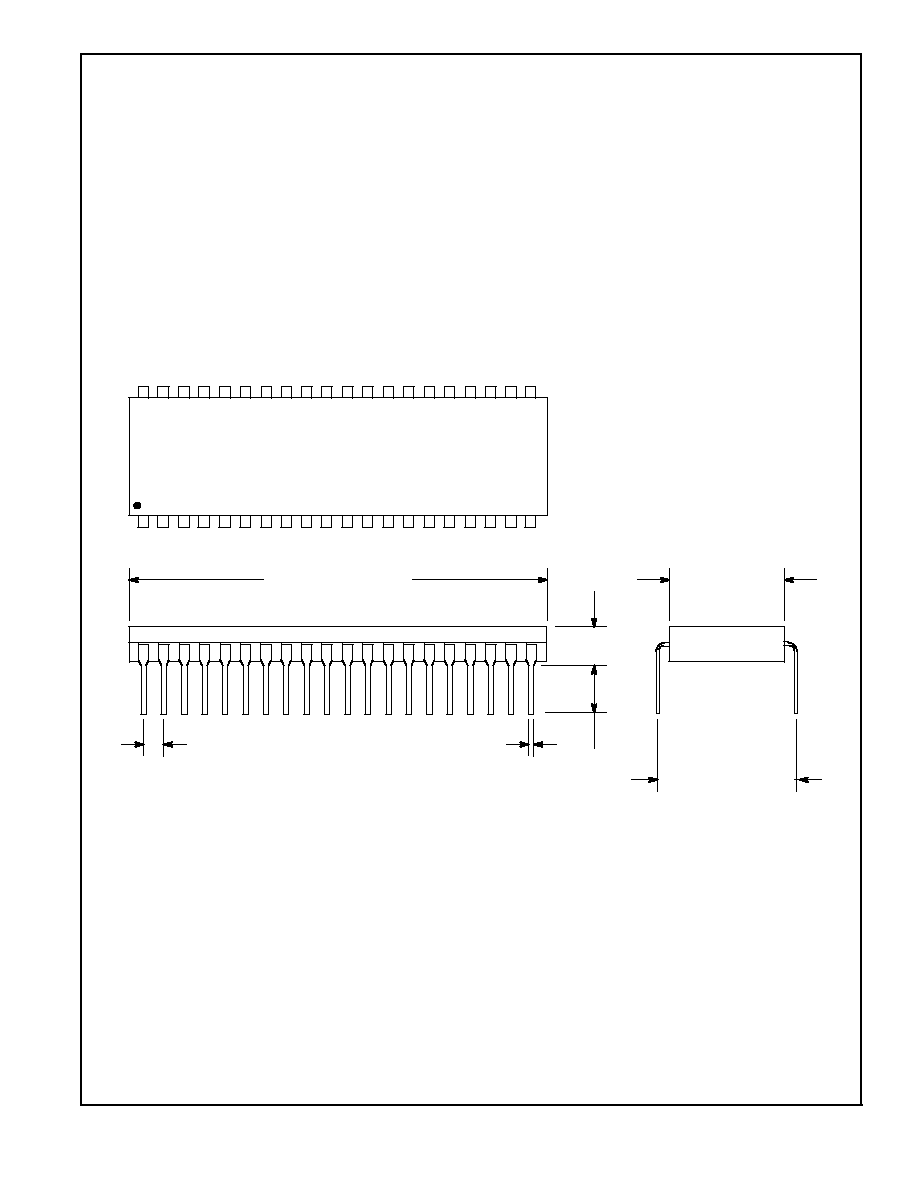
utilizes N channel silicon gate depletion load technology and is packaged in a 40ŁLead DIP type package.
Features:
D
Two Independent 8ŁBit Bidirectional Peripheral Interface Ports with "Handshake" Data Transfer
Control
D
Interrupt Driven "Handshake" for Fast Response
D
Any One of Four Distinct Modes of Operation may be Selected for a Port, including:
Byte Output
Byte Input
Byte Bidirectional Bus (Available on Port A Only)
Bit Control Mode
D
All with Interrupt Controlled Handshake
D
Daisy Chain Priority Interrupt Logic Included to Provide for Automatic Interrupt Vectoring without
External Logic
D
Eight Outputs are Capable of Driving Darlington Transistors
D
All Inputs and Outputs Fully TTL Compatible
D
Single 5 Volt Supply and Single Phase Clock Required
Absolute Maximum Ratings:
Temperature Under Bias
0
░
to +70
░
C
. . . . . . . . . . . . . . . . . . . . . . . . . . . . . . . . . . . . . . . . . . . . . . . . . . . . .
Storage Temperature Range
Ł65
░
to +150
░
C
. . . . . . . . . . . . . . . . . . . . . . . . . . . . . . . . . . . . . . . . . . . . . . .
Voltage On Any Pin With Respect to GND
Ł0.3V to +7V
. . . . . . . . . . . . . . . . . . . . . . . . . . . . . . . . . . . . .
Power Dissipation
6W
. . . . . . . . . . . . . . . . . . . . . . . . . . . . . . . . . . . . . . . . . . . . . . . . . . . . . . . . . . . . . . . . . .
Note 1. Stresses above those listed under "Absolute Maximum Ratings" may cause permanent
damage to the device. This is a stress rating only functional operation of the device at these
or any other condition above those indicated in the operational sections of this specification
is not implied. Exposure to absolute maximum rating conditions for extended periods may
affect device reliability.

DC Characteristics: (T
A
= 0
░
to 70
░
C, V
CC
= 5V
▒
5% unless otherwise specified)
Parameter
Symbol
Test Conditions
Min
Typ
Max
Unit
Clock Input Low Voltage
V
ILC
Ł0.3
Ł
0.80
V
Clock Input High Voltage
V
IHC
V
CC
Ł0.6
Ł
V
CC
+3
V
Input Low Voltage
V
IL
Ł0.3
Ł
0.8
V
Input High Voltage
V
IH
2.0
Ł
V
CC
V
Output Low Voltage
V
OL
I
OL
= 2.0mA
Ł
Ł
0.4
V
Output High Voltage
V
OH
I
OH
= Ł250
Ą
A
2.4
Ł
Ł
V
Power Supply Current
I
CC
Ł
Ł
70
mA
Input Leakage Current
I
L1
V
IN
= 0 to V
CC
Ł
Ł
▒
10
Ą
A
TriŁState Output Leakage Current in Float
I
LOH
V
OUT
= 2.4 to V
CC
Ł
Ł
10
Ą
A
TriŁState Output Leakage Current in Float
I
LOL
V
OUT
= 0.4V
Ł
Ł
Ł10
Ą
A
Data Bus Leakage Current in Input Mode
I
LD
0
V
IN
V
CC
Ł
Ł
▒
10
Ą
A
Darlington Drive Current
I
OHD
V
OH
= 1.5V Port B Only
Ł1.5
Ł
Ł
mA
Capacitance: (T
A
= +25
░
C, f = 1MHz unless otherwise specified)
Parameter
Symbol
Test Conditions
Min
Typ
Max
Unit
Clock Capacitance
C
Unmeasured Pins
Ł
Ł
10
pF
Input Capacitance
C
IN
Input Capacitance
Ł
Ł
5
pF
Output Capacitance
C
OUT
Ł
Ł
10
pF
AC Characteristics: (T
A
= 0
░
to 70
░
C, V
CC
= 5V
▒
5% unless otherwise specified)
Parameter
Symbol
Test Conditions
Min
Typ
Max
Unit
Clock Cycle Time
TcC
Note 1
250
Ł
Ł
ns
Clock Width (High)
TcCH
105
Ł
2000
ns
Clock Width (Low)
TcCL
105
Ł
2000
ns
Clock Fall Time
TfC
Ł
Ł
30
ns
Clock Rise Time
TrC
Ł
Ł
30
ns
CE, B/A, C/E, to RD, IORQ
Setup Time
TsCS(RI)
Note 2
50
Ł
Ł
ns
Any Hold Time for Specified Setup Time
Th
0
Ł
Ł
ns
RD, IORQ to Clock
Setup Time
TsRI(C)
115
Ł
Ł
ns
RD, IORQ
to Data Out Delay
TdRI(DO)
Note 3
Ł
Ł
380
ns
RD, IORQ
to Data Out Float Delay
TdRI(DOr)
Ł
Ł
110
ns
Data In to Clock
Setup Time
TsDI(C)
C
L
= 50pF
50
Ł
Ł
ns
IORQ
to Data Out Delay (INTA Cycle)
TdIO(DOI)
Note 4
250
Ł
Ł
ns
M1
to Clock
Setup Time
TsM1(Cr)
90
Ł
Ł
ns
M1
to Clock
Setup Time (M1 Cycle)
TsM1(Cf)
0
Ł
Ł
ns
Note 1 TcC = TwCh + TwCI + TrC + TfC.
Note 2. TsCS(RI) may be reduced. However, the time subtracted from TsCS(RI) will be added to
TdR(DO).
Note 3. Increase TdRI(DO) by 10ns for each 50pF increase in loading up to 200pF max.
Note 4. Increase TdIO(DOT) by 10ns for each 60pF increase in loading up to 200pF max.

AC Characteristics (Cont'd): (T
A
= 0
░
to 70
░
C, V
CC
= 5V
▒
5% unless otherwise specified)
Parameter
Symbol
Test Conditions
Min
Typ
Max
Unit
M1
to IEO
Delay (Interrupt Immediately
Preceding M1)
TdM1(IEO)
Note 5, Note 6
Ł
Ł
190
ns
IEI to IORQ
Setup Time (INTA Cycle)
TsIE(IO)
Note 6
140
Ł
Ł
ns
IEI
to IEO
Delay
TdIEI(IEO)
C
L
= 50pF, Note 5
Ł
Ł
130
ns
IEI
to IEO
Delay (after ED Decode)
TdIE(IIOr)
Note 5
Ł
Ł
160
ns
IORQ
to Clock
Setup Time (To Activate
READY on Next Clock Cycle)
TsIO(C)
220
Ł
Ł
ns
Clock
to Ready
Delay
TdC(RDYr)
C
L
= 50pF, Note 5
200
Ł
Ł
ns
Clock
to Ready
Delay
TdC(RDYf)
Note 5
150
Ł
Ł
ns
STROBE Pulse Width
TwSTB
Note 4
150
Ł
Ł
ns
STROBE
to Clock
Setup Time (To Activate
READY on Next Clock Cycle)
TsSTB(C)
200
Ł
Ł
ns
IORQ
to PORT Data Stable Delay (Mode 0)
TdIO(PD)
Note 5
Ł
Ł
180
ns
PORT DATA to STROBE
Setup Time (Mode 1)
TsPD(STB)
230
Ł
Ł
ns
STROBE
to PORT DATA Stable (Mode 2)
TdSTB(PD)
Note 5
Ł
Ł
210
ns
STROBE
to PORT DATA Float Delay (Mode 2)
TdSTB(PDz) C
L
= 50pF
Ł
Ł
180
ns
PORT DATA Match to INT
Delay (Mode 3)
TdPD(INT)
Ł
Ł
490
ns
STROBE
to INT
Delay
TdSTB(INT)
Ł
Ł
440
ns
Note 4 For Mode 2: t
W(ST)
>
t
S(PD)
Note 5 Increase these values by 2nsec for each 10pF increase in loading up to 100pF max.
Note 6. 2.5 TcC > (NŁ2) TdIEI (IEOG) + TdM1(IEO) + TsIE(IO) + TTL Buffer Delay, if any.
INT
B
7
RD
IORQ
M1
D
5
D
4
D
3
A STB
Chip Enable
Pin Connection Diagram
B
0
B
1
B
2
B
3
B
4
B
5
B
6
B STB
GND
B RDY
IEO
IEI
System Clock Input
(+) 5V
1
2
3
4
5
Control Data Select
6
Port B/A Select
7
8
40
39
38
37
36
35
34
33
9
32
10
11
31
30
12
29
13
28
14
27
A RDY
15
26
16
17
25
24
18
23
19
22
20
21
D
0
D
1
D
2
D
7
D
6
A
7
A
6
A
5
A
4
A
3
A
2
A
1
A
0