Copyright 1998 National Semiconductor Corp.
1
www.national.com
SC14422
Complete Baseband Processor for DECT Base Stations
General Description
Preliminary document version 1.1.
The SC14422 is a 3.0 Volt CMOS IC optimized to handle
all the audio, signal and data processing needed within a
DECT basestation. An ADPCM transcoder, a very low
power CODEC and Analog Frontend are integrated. Di-
rect connections towards analog or ISDN line interface.
The SC14422 is designed to be compatible with many
radio interfaces. A dedicated TDMA controller handles all
physical layer slot formats and radio control.
The integrated National Semiconductor's standard
CR16A processor core with external Program memory
(Flash or ROM) takes care of all the higher protocol stack.
Programmable I/O ports can be configured as chip selects
for I/O expanders, Serial Flash memory, interrupt source
or I/O. A digital serial interface can be configured to inter-
face to many codecs and ISDN devices with
µ
-Law, a-Law,
linear or transparent data formats.
Features
s
Integrated DECT base band transceiver optimized for
GAP base stations according to ETS 300 175-2, 175-3
& 175-8.
s
3.0 to 5.5 Volt operating voltage.
s
Embedded 16 bit CompactRISC
TM
CR16A Microproc-
essor with In System Emulation (ISE) mode.
s
2k + 4kbyte Data Memory.
s
Two full duplex 32 kbits/sec ADPCM transcoder.
s
14-bit linear CODEC with programmable gain
s
Serial interface to external codecs and ISDN interface
circuits.
s
Echo canceller, two echo suppressors, DTMF genera-
tor, sidetone and artificial echo loss.
s
On-chip gaussian Modulator.
s
Peak hold ADC for RSSI measurement
s
Three input 8 bit successive approximation ADC.
s
On board programmable Dedicated Instruction Proces-
sor (DIP) for all TDMA based events.
s
Protected and unprotected half, full and double slot B-
fields D00, D08, D32 and D80
s
Standard DECT encryption with different keys for
different MAC-connections.
s
6 MAC connections can be handled simultaneously.
s
Flexible three wire interface to radio front synthesizer.
s
Three general purpose I/O ports with programmable in-
terrupts.
s
General purpose full duplex UART.
s
SPI
TM
and MICROWIRE
TM
interfaces.
s
Two general purpose timers and watchdog timer.
s
Programmable chip selects to 8 bit wide ROM, SRAM
NAND Flash Memory and I/O expanders.
s
Capture timer for frequency measurement for e.g. me-
tering, ringing and call progress tone detection.
s
100 pin TQFP-100 package.
________________________________________________________________________________________________
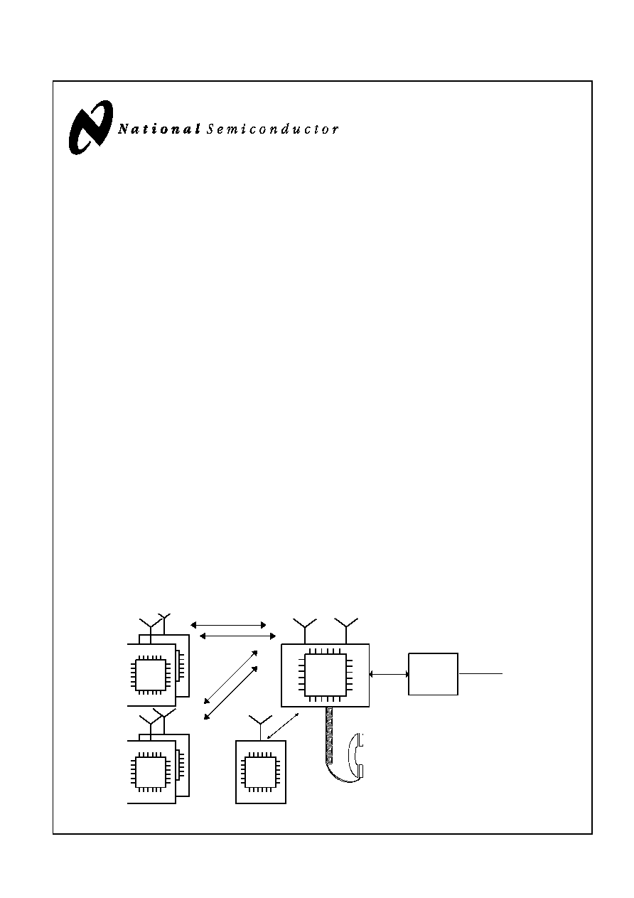
System Diagram
SC14401
SC14402
SC14401
4220030
SC14402
SC14402
SC14422
PSTN
ISDN
ISDN or
PSTN
Interface
PRELIMINARY
March 1998
S
C
1
4
4
2
2
C
o
m
p
l
e
t
e
B
a
s
e
b
a
n
d
P
r
o
c
e
s
s
o
r
f
o
r
D
E
C
T
B
a
s
e
S
t
a
t
i
o
n
s
SPI
TM
is a trademark of Motorola, MICROWIRE
TM
and CompactRISC
TM
are trademarks of National Semiconductor Corporation

Table of Contents
Copyright 1998 National Semiconductor Corp.
2
www.national.com
1.0 CONNECTION DIAGRAM . . . . . . . . . . . . . . . . . . . . . 3
2.0 PIN DESCRIPTION . . . . . . . . . . . . . . . . . . . . . . . . . . . 4
Copyright 1998 National Semiconductor Corp.
3
www.national.com
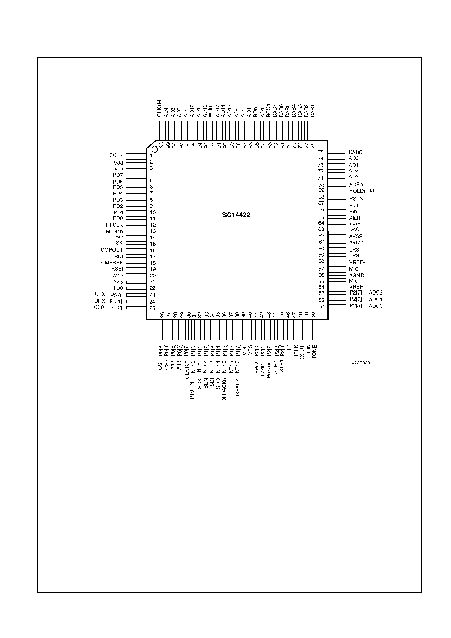
1.0 Connection Diagram
Order Number SC14422VJG (Standard version)
Order Number SC14422RVJG (`R' Version works with RTX-GAP Software)
See NS Package Number VJG100A

Copyright 1998 National Semiconductor Corp.
4
www.national.com
2.0 Pin Description
Table 1:
Pin Description)
PIN NAME
NR
TYPE
DESCRIPTION
SCLK
1
1
OUTPUT/INPUT. CR16A bus interface System CLocK output. In core mode this pin
is input.
VDD
2
Digital supply voltage
VSS
3
Digital ground
PD
7..0
4-11
5
TRI-STATE OUTPUT. Programmable Power Down pins 7 to 0 to radio interface.
PD7,6 have 12 mA drive.
RFCLK
12
5b
OUTPUT (Slope controlled). 10.368 MHz clock output. Logic `0' after reset or when
disabled.
MEN1n
13
5
OUTPUT. Programmable Load Enable for synthesizer. Can be synchronized to
LKD input.
SO
14
1
TRI-STATE OUTPUT. Serial data output.
SK
15
5
OUTPUT. Serial interface clock: 1.152 MHz
CMPOUT
16
1
TRI-STATE OUTPUT. Comparator output pin.
RDI
17
analog
INPUT. Received Data. The polarity of this input is programmable.
CMPREF
18
analog
INPUT. Comparator reference level. Internally a six bit DAC can be connected to
this pin to compensate for DC offsets.
RSSI
19
analog
INPUT. Receiver Signal Strength Indication. This signal is connected to a 6-bit ADC
input with peak hold circuitry. PD0 internally controls the peak hold circuitry. If PD0
is low RSSI is sampled, else the RSSI input will be connected to ground.
AVD
20
Analog supply voltage.
AVS
21
Analog ground.
TDO
22
5/analog
TRI-STATE OUTPUT. Transmit Data. The polarity of this output is programmable.
P0[0] or
UTX
23
2
INPUT/OUTPUT with selectable pull up resistor. General purpose memory
mapped I/O port bit. UART data output.
P0[1] or
URX
24
3
INPUT/OUTPUT with selectable pull down resistor. General purpose memory
mapped I/O port bit. UART data input.
P0[2] or
CS0
25
2
INPUT/OUTPUT with selectable pull up resistor. General purpose memory
mapped I/O port bit. Multi function Chip select output CS0
P0[3] or
CS1
26
2
INPUT/OUTPUT with selectable pull up resistor. General purpose memory
mapped I/O port bit. Multi function Chip select output CS1
P0[4] or
CS2
27
2
INPUT/OUTPUT with selectable pull up resistor. General purpose memory
mapped I/O port bit. Multi function Chip select output CS2
P0[5] or
AD18
28
3
INPUT/OUTPUT with selectable pull down resistor. General purpose memory
mapped I/O port bit. OUTPUT Address bit 18.
P0[6] or
AD19
29
3
INPUT/OUTPUT with selectable pull down resistor. General purpose memory
mapped I/O port bit. OUTPUT Address bit 19.
P0[7] or
CLK100
30
2
INPUT/OUTPUT with selectable pull up resistor. General purpose memory
mapped I/O port bit. OUTPUT 100 Hz clock synchronized to 10 msec frame.
P1[0] or
P10_INT
31
2
INPUT/OUTPUT with selectable pull up resistor. General purpose memory
mapped I/O port bit. Level sensitive interrupt source P10_INT
P1[1] or
SCK
32
2
INPUT/OUTPUT with selectable pull up resistor. General purpose memory
mapped I/O port bit. SPI Clock input/output
P1[2] or
SEN
33
2
INPUT/OUTPUT with selectable pull up resistor. General purpose memory
mapped I/O port bit. SPI Clock enable input if SPI slave. If SPI master this pin must
be set/reset by software.
P1[3] or
SDI
34
2
INPUT/OUTPUT with selectable pull up resistor. General purpose memory
mapped I/O port bit. SPI data input
P1[4] or
SDO
35
2
INPUT/OUTPUT with selectable pull up resistor. General purpose memory
mapped I/O port bit. SPI data output

Copyright 1998 National Semiconductor Corp.
5
www.national.com
P1[5] or
HOLDACKn
36
2
INPUT/OUTPUT with selectable pull up resistor. General purpose memory
mapped I/O port bit. This pin can be configured as active low HOLD acknowledge.
In Emulation mode HOLDACKn is automatically selected.
P1[6] or
ISE
37
2
INPUT/OUTPUT with selectable pull up resistor. General purpose memory
mapped I/O port. In development mode this pin generates an ISE interrupt to the
CR16A core if high.
P1[7] or
READY
38
4
INPUT/OUTPUT with open drain with 100 mA sink capability. If P1[7] is configured
as READY pin then if HOLDn is `1', this pin will become low upon a read or write
access by an external processor. Can be used to control a LED connected to VDD..
VDD
39
Digital supply voltage.
VSS
40
Digital ground.
P2[0] or
PWM
41
4
INPUT/OUTPUT with open drain with 100mA sink capability. This pin can also be
configured as single ended buzzer driver.
P2[1] or
Buzzer+
42
1
INPUT/OUTPUT. General purpose memory mapped I/O port bit. P2[1,2] can be
configured as complementary PWM output for e.g. buzzer control. P2[1,2] can
drive 12 mA.
P2[2] or
Buzzer-
43
1
INPUT/OUTPUT. General purpose memory mapped I/O port bit. P2[1,2] can be
configured as complementary PWM output for e.g. buzzer control. P2[1,2] can
drive 12 mA.
P2[3] or
STR0
44
1
INPUT/OUTPUT. General purpose memory mapped I/O port bit.
OUTPUT External interface strobe 0.
P2[4] or
STR1
45
1
INPUT/OUTPUT. General purpose memory mapped I/O port bit.
INPUT/OUTPUT. External interface strobe STR1.
TP
46
1
INPUT. Testpin
ICLK
47
1
INPUT/OUTPUT. External interface clock. On rising edge data is valid.
COUT
48
4
INPUT/OUTPUT. External interface data input, codec output. If output, this pin is
configured as an open drain. If the internal codec is used (format 1) an external pull
up resistor is required.
CIN
49
1
INPUT/OUTPUT. PCM interface data output, codec input
TONE
50
1
INPUT. TONE input to capture timer (e.g. metering tones)
P2[5] or
ADC0/DAC0
51
5/analog
DIGITAL OUTPUT/ANALOG INPUT. General purpose input to 8 bit ADC. 8 bit DAC
if ADC0,1,2 are not selected. P2[5] can also be used as a digital output.
P2[6] or
ADC1
52
5/analog
DIGITAL OUTPUT/ANALOG INPUT. General purpose input one to 8 bit ADC
P2[6] can also be used as a digital output.
P2[7] or
ADC2
53
5/analog
DIGITAL OUTPUT/ANALOG INPUT. General purpose input two to 8 bit ADC.
P2[7] can also be used as a digital output.
Vref+
54
analog
OUTPUT. Positive microphone reference voltage.
MIC+
55
analog
INPUT. Microphone positive input.
AGND
56
analog
Signal ground output.
MIC-
57
analog
INPUT. Microphone negative input.
Vref-
58
analog
OUTPUT. Negative microphone reference voltage.
LRS-
59
analog
OUTPUT. Negative loudspeaker output.
LRS+
60
analog
OUTPUT. Positive loudspeaker output
AVD2
61
Analog supply.
AVS2
62
Analog ground.
DAC
63
analog
OUTPUT. 8 bit DAC output e.g. for frequency control
CAP
64
analog
External capacitor for crystal oscillator.
Xtal1
65
analog
INPUT. 10.368 MHz crystal connection.
VSS
66
Digital ground.
VDD
67
Positive supply voltage.
Table 1:
Pin Description)
PIN NAME
NR
TYPE
DESCRIPTION